
Automotive signal ICs routinely face -40°C to 125°C operation windows and stringent AEC‑Q100 qualification; this article turns the part datasheet into actionable guidance for in‑vehicle designs. The intent is practical: extract electrical limits, thermal behavior, and test cases so engineers can map device parameters to system choices quickly. The write‑up highlights datasheet numbers, design implications, and bench/field validation steps for comparator‑class interfaces used across body, power, and safety domains.
1 — Overview: What the TLV3232QDGKRQ1 Offers for Automotive Designs
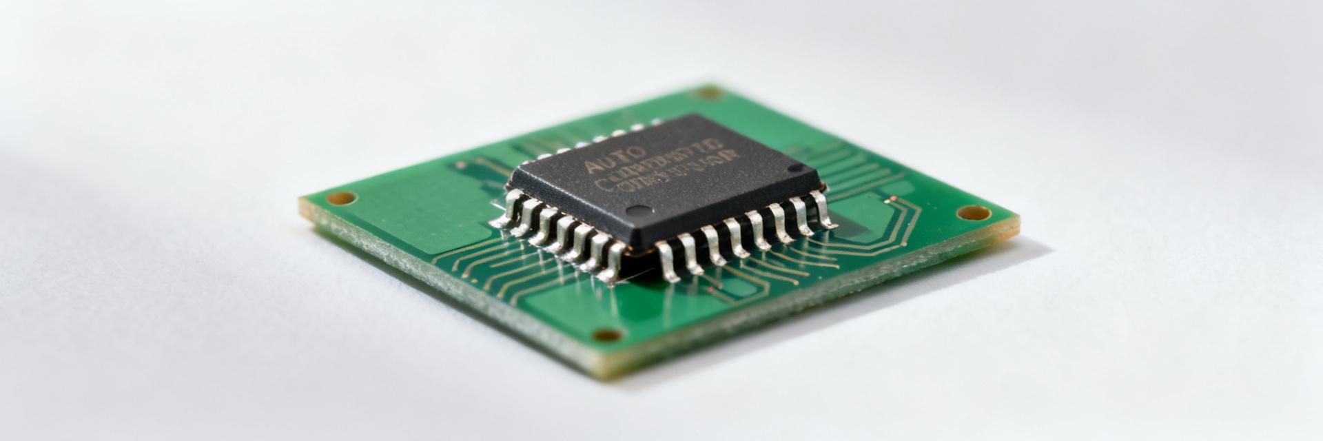
— Device role and common automotive applications
Point: This device is a low‑power comparator/analog interface optimized for sensor thresholds and wake circuits. Evidence: per the device class, it provides push‑pull outputs and low quiescent current typical of micropower comparators. Explanation: Engineers commonly use it for window detection on temperature or light sensors, microcontroller wake‑up from low‑power domains, and simple diagnostic thresholds in body electronics and auxiliary subsystems.
— Package, temperature grade and qualification highlights
Point: The part ships in small, automotive‑grade surface‑mount packages suitable for compact boards. Evidence: it is specified for extended automotive temperature operation and AEC‑level qualification. Explanation: That qualification and the -40°C to 125°C operating window reduce supplier risk for long‑life fleets and imply traceability and manufacturing controls that ease procurement for Tier‑1 BOMs while affecting footprint and reflow profiles on the PCB.
2 — Key Electrical Specifications from the TLV3232QDGKRQ1 Datasheet
— Power, I/O and bias specifications (numbers + design impact)
Point: Supply range and quiescent power are primary constraints for system power budgeting. Evidence: the comparator supports a wide supply window up to 5.5V and exhibits single‑digit microamp quiescent currents per datasheet typical values. Explanation: Designers can interface directly with 3.3V or 5V domains using level‑aware outputs; battery/ignition scenarios should budget quiescent current times expected standby hours to project drain and choose rail sequencing to avoid latch‑up.
— Performance metrics: offset, bias current, propagation delay, common-mode range
Point: Offset, input bias, delay and common‑mode limits determine accuracy and timing margins. Evidence: typical input offset is a few millivolts, input bias in low nA range, and propagation delays in the 10s of ns per channel per datasheet. Explanation: For a 4 mV offset, threshold hysteresis and comparator trip margins should increase by several millivolts; for timing, add worst‑case propagation to debounce and state‑machine windows to avoid false triggers.
| Parameter | Typical / Max Value |
|---|---|
| Supply voltage | 1.8 V – 5.5 V |
| Quiescent current (per device) | Low µA range (typical) |
| Input offset | ~1–5 mV (typ) |
| Propagation delay | ~40 ns (order) |
| Input common‑mode | Includes rail‑to‑within a few hundred mV |
3 — Thermal, Reliability & Qualification Details
— Thermal behavior and PCB-level thermal management
Point: Thermal resistance and power dissipation set junction rise in hot cabins and engine compartments. Evidence: device dissipation is small, but ambient can exceed 85°C in confined enclosures, so PCB thermal plan matters. Explanation: Use copper pours, thermal vias, and short power traces to lower θJA; perform a worst‑case junction estimate (TJ = TA + θJA × Pdiss) and derate margin for repeated high‑ambient soak conditions.
— Reliability considerations & qualification tests to expect
Point: Expect standard automotive stress screens and electrical robustness reports. Evidence: qualification includes temperature cycling, HTRB/HAST and defined ESD/EMC limits consistent with automotive specs. Explanation: Request supplier test summaries (lot traceability, stress test results) and plan in‑house samples for HAST, ESD and EMC pre‑compliance checks before committing to long‑lead programs.
4 — Integration & Design Guidance for Automotive Systems
— Power supply decoupling, filtering and layout best practices
Point: Proper decoupling and placement prevent transients from corrupting comparator thresholds. Evidence: datasheet recommends local bypass close to VCC pin with a low‑ESR ceramic and additional bulk caps. Explanation: Place a 0.1 µF ceramic within 1–2 mm of the supply pin, add a 1–10 µF bulk cap for load dump resilience, and route ground returns directly to a quiet analog ground to minimize common‑impedance coupling.
— Input protection, ESD/EMI and fault handling
Point: Automotive inputs require transient suppression to survive load dumps and ESD. Evidence: input common‑mode and input clamp behavior limit safe external voltages. Explanation: Add TVS diodes sized for expected clamp energy, a series resistor to limit input current, and consider Pi filtering for EMI; select protection components based on expected peak amplitude and response time to avoid slowing the comparator unacceptably.
5 — Practical Checklist & Test Cases to Validate TLV3232QDGKRQ1 in Vehicles
— Bench tests mapped to datasheet limits
Point: Create a focused bench matrix that stresses each datasheet limit. Evidence: include supply sweep, input common‑mode sweep, temperature box runs, offset drift and propagation timing under load. Explanation: Define pass/fail using datasheet max/typ values, use a scope with 1–2 ns/div for timing, and verify thresholds across rails and temperatures; record raw traces for supplier escalation if margins fail.
— Field validation and long-term monitoring recommendations
Point: In‑vehicle testing uncovers age and environment effects not seen on bench. Evidence: plan soak tests, event logging for overvoltage/ESD, and periodic offset checks. Explanation: Log offset drift and error counts across months, set automated alerts for drift beyond tolerance, and have escalation criteria (e.g., drift > 2× datasheet drift) to trigger supplier return or redesign.
Summary
- The TLV3232QDGKRQ1 combines low quiescent current, small input offset, and automotive qualification, making it suitable for wake, window detect and sensor interface functions; designers should map these figures to trip margins and power‑budget calculations.
- Key electricals—supply range to 5.5V, µA‑class standby, millivolt offsets and sub‑100 ns delays—drive rail selection and hysteresis strategy; reference datasheet limits when sizing filters and protection.
- Thermal and reliability practices—copper pours, thermal vias, and targeted qualification checks—ensure the device meets automotive specs in high ambient and long‑life installations.
6 — Frequently Asked Questions
How should engineers use the datasheet to set comparator thresholds?
Base thresholds on typical offset plus margin. With a typical offset of a few millivolts and possible drift across temp, set threshold margins at least 2–3× the typical offset plus expected drift; include hysteresis where contact bounce or noise could cause chatter and validate across -40°C to 125°C.
What decoupling is recommended for stable TLV3232QDGKRQ1 operation?
Local high‑frequency and bulk decoupling stabilize the rail during transients. Placing a 0.1 µF ceramic capacitor within 1–2 mm of the supply pin, keeping traces short, and adding a low‑ESR bulk capacitor nearby helps handle load dumps and source-impedance fluctuations.
Which bench tests best reveal real‑world failures versus datasheet limits?
Combined stress tests emulate field conditions. Running supply sweeps and input common‑mode range sweeps at temperature extremes (-40°C, 25°C, and 125°C) reveals margin erosion, allowing engineers to verify offset drift and timing metrics before committing to mass production.
Why is hysteresis critical for the TLV3232QDGKRQ1 in automotive sensor applications?
In vehicle environments, high electromagnetic noise, battery rail transients, and slowly changing sensor inputs can cause comparator outputs to chatter near the threshold. Implementing external positive feedback hysteresis stabilizes the transition state, protecting downstream MCUs from invalid high-frequency interrupts.





