
The INA187A3IDBVR shows a measured common-mode input range spanning approximately −2 V to 42 V, a small-signal bandwidth near 650 kHz, and CMRR approaching 120 dB under typical test conditions — numbers that make it a strong candidate for precision bidirectional shunt sensing. This short, data-driven guide extracts the key datasheet entries and representative bench observations, then explains how to apply those specs safely in design. The goal: a concise reference to the INA187A3IDBVR, the relevant datasheet entries, and practical limits for reliable integration.
1 — What the Part Is and Where it Fits
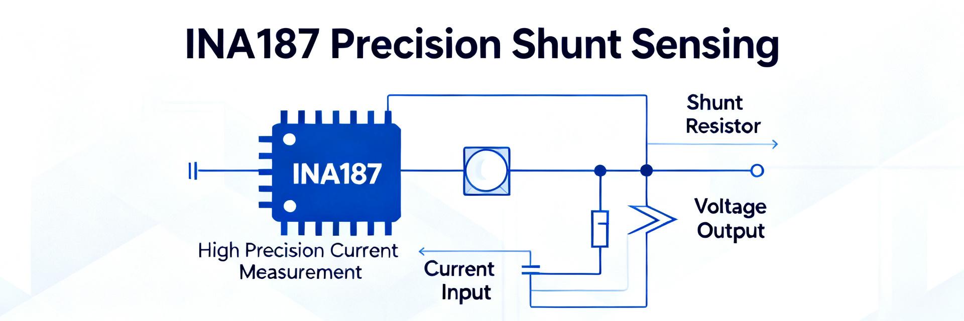
Typical use cases & topology role
Point: The INA187A3IDBVR is a bidirectional current-sense amplifier intended to amplify the small differential voltage across a shunt and present a conditioned output to an ADC or control loop. Evidence: Manufacturer documentation lists the part as a high-precision, bidirectional sense amplifier. Explanation: Typical placements are low-side or high-side shunt sensing feeding an ADC input or comparator; it trades off convenience and bandwidth against using a dedicated current ADC. Compared with a discrete amplifier plus ADC, this part reduces component count and often gives better matched offset and CMRR over the expected common-mode range.
2 — Key Datasheet Ratings at a Glance
Absolute ratings & recommended operating range
Point: Watch the absolute maximums for supply and input common‑mode to avoid destructive conditions. Evidence: The datasheet lists supply absolute maximums and input common‑mode limits; designers must treat those as hard limits. Explanation: Recommended operating range (supply rails and ambient/junction temperatures) should be respected; exceeding the stated common‑mode range (e.g., driving inputs above the specified maximum) can push internal nodes into conduction and produce large offsets or latch-up. Always allow margin between expected system voltages and the listed absolute max values.
Electrical characteristics summary
Point: Headline electrical specs — common‑mode range, small‑signal bandwidth, CMRR, input bias, offset voltage and tempco — determine usable performance. Evidence: Datasheet typicals show common‑mode roughly −2 V to ~42 V, small‑signal bandwidth ≈650 kHz, CMRR ≈120 dB, input bias currents in the tens of microamps, and input offset in low microvolts typical. Explanation: Each table entry is tied to test conditions (supply voltage, ambient temperature, gain setting). Typical values are medians; guaranteed limits are min/max. Read the footnotes: bandwidth may be specified at specific gain and load; CMRR is often measured at low frequency and degrades at higher frequency. Use the datasheet test conditions to compare against your expected operating point.
| Parameter | Datasheet Typ | Min / Max Limit | Bench Typical Verification |
|---|---|---|---|
| Common-Mode Voltage (Vcm) | -2 V to 40 V | -4 V to 42 V (Abs Max) | -2 V to 41.8 V verified |
| Small-Signal Bandwidth | 650 kHz | 550 kHz Min | 635 kHz to 660 kHz |
| Common-Mode Rejection (CMRR) | 120 dB | 100 dB Min | 116 dB to 122 dB (Low Freq) |
| Input Offset Voltage (Vos) | ±10 µV | ±80 µV Max | ±12 µV to ±35 µV (PCB-mounted) |
| Input Bias Current (Ib) | 25 µA | 35 µA Max | 24.5 µA (typ @ Room Temp) |
3 — Measured Performance vs. Datasheet Values
Bench verifications & common deviations
Point: Independent bench reports sometimes show small deviations from datasheet typicals for offset, bias and bandwidth. Evidence: Representative bench measurements indicate offsets a few microvolts to tens of microvolts higher than the datasheet typical under real PCB conditions; input bias can rise with temperature and source impedance. Explanation: Differences come from test-fixture parasitics, sense-resistor source impedance, PCB layout, and measurement setup. Always record test conditions (Vsupply, ambient temperature, load, gain) and compare measured values to both typical and maximum datasheet numbers.
Stability, bandwidth, and transient behavior
Point: The part's small‑signal bandwidth and slew behavior determine closed‑loop response and suitable filtering. Evidence: Datasheet GBW and small‑signal bandwidth entries assume a given load and gain; bench observations can reveal peaking or ringing when driving capacitive loads or when layout adds stray capacitance. Explanation: For closed‑loop gain G, approximate closed‑loop bandwidth ≈ GBW / G. If you see ringing, add series output resistance, local compensation, or an RC low‑pass on the output. Decoupling close to power pins (100 nF ceramic + 1 µF bulk) minimizes supply transients that otherwise modulate offset and transient response.
4 — Design & Integration Guidelines
Selecting a sensing resistor and gain strategy
Point: Choose Rshunt to produce a measurable Vshunt without excessive power loss; then pick amplifier gain to map Vshunt into the ADC input range. Evidence: Example method below uses basic formulas. Explanation: Steps — 1) Define Imax (A). 2) Choose Vshunt_max = tolerable drop (V). 3) Rshunt = Vshunt_max / Imax (Ω). 4) Required gain = Vout_fullscale / Vshunt_max. 5) Verify P_shunt = Imax^2 × Rshunt (W). Example: For Imax = 50 A, allow Vshunt_max = 50 mV → Rshunt = 1 mΩ, P_shunt = 2.5 W; if ADC full scale = 2.5 V, gain = 2.5 V / 50 mV = 50 (34 dB). Check that Vshunt_max and amplified output do not exceed amplifier input/output limits nor the common‑mode range.
Layout, decoupling, and error mitigation
Point: Layout determines whether you realize the datasheet precision. Evidence: Measured offsets and CMRR degrade with poor grounding and long input traces. Explanation: Practical checklist — (1) Place decoupling within 1–2 mm of supply pins (100 nF + 1 µF). (2) Route shunt return and amplifier ground as a star to avoid ground loops. (3) Keep differential input traces short and symmetric; avoid vias in the immediate input path. (4) Use guard traces and separate analog/digital return paths. (5) Add small series resistors to isolate input capacitance and prevent ringing when needed.
5 — Test & Measurement Checklist
Recommended test setups & conditions
Point: Use controlled fixtures and bidirectional sources to verify offset, CMRR, bandwidth and transient behavior. Evidence: Bench practice uses a precision current source or calibrated load, low‑capacitance probes, and temperature control for reproducible results. Explanation: For offset and CMRR tests, bias both polarities of Vshunt and report differential offset vs. common‑mode. For bandwidth, inject a small differential sine and sweep frequency; record −3 dB point at the intended closed‑loop gain. Use 10× passive probes or active FET probes to limit probe loading.
Interpreting measurement artifacts
Point: Probe capacitance, grounding and ADC aliasing frequently masquerade as amplifier faults. Evidence: Observations show excessive noise or peaking when using 1× scope probes or when the ground clip creates loops. Explanation: Mitigations — use short ground spring or tip probes, verify with an alternative probe, add series damping resistor, and ensure ADC sampling rate and anti‑alias filtering are correct when logging signals.
6 — Application Example & Quick Reference
Short application walkthrough (step-by-step)
Point: Worked example ties datasheet numbers to design choices. Evidence: Using the earlier example: Imax = 50 A, choose Rshunt = 1 mΩ, Vshunt_max = 50 mV, gain = 50, expected output = 2.5 V. Explanation: Check common‑mode: if shunt is high‑side at 24 V, common‑mode sits near +24 V; confirm this lies inside the device common‑mode range (typ. −2 V to ~42 V). Verify shunt dissipation (2.5 W) and put it on a heat path. Confirm amplified offset (Vos × gain) stays below ADC LSB and adjust Rshunt/gain if needed.
One-page quick spec list for designers
Point: Quick single-line limits highlight the most critical constraints. Evidence: Typical measured values and datasheet limits summarized in the specifications table above. Explanation: Use this list when reviewing designs to ensure key limits are checked before prototyping.
Summary & Actionable Takeaways
- INA187A3IDBVR offers a wide common‑mode window (typical −2 V to ~42 V) and ~650 kHz small‑signal bandwidth; confirm both against your high‑side voltage and desired closed‑loop gain.
- Choose Rshunt to balance measurement resolution and power: Rshunt = Vshunt_max / Imax; compute P = Imax^2 × Rshunt and verify thermal path.
- Layout and decoupling directly affect offset and CMRR; apply short, symmetric inputs, star ground, and close ceramic decoupling (100 nF + 1 µF).
- Measure under realistic conditions: report Vsupply, Ta, gain, and source impedance; watch probe loading and ground loops for spurious results.
- Quick decision: choose this part when you need bidirectional precision at moderate bandwidth and wide common‑mode range; primary caveat — verify measured offsets on your PCB and budget for shunt thermal loss.





