
Introduction: Bench measurements establish practical expectations for the INA299A1IDBVR: small-signal bandwidth measured at or above 650 kHz, quiescent current near 650 μA typical, and reliable operation across roughly 2.7 V up to about 12 V in common lab setups. This introduction sets the stage to compare datasheet listings with observed bench behavior and practical design implications.
The goal is pragmatic: reconcile datasheet entries with real measurements, highlight critical specs and absolute limits you must respect, and provide test procedures and layout checks to reproduce results. Emphasis is on accuracy, reproducibility, and actionable guidance engineers can apply when integrating this single-chip current-sense amplifier into power or telemetry subsystems.
1 — Quick overview: what the INA299A1IDBVR is and the headline specs (background)
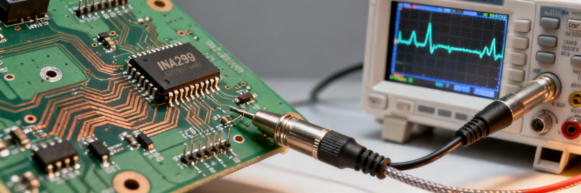
1.1 Device role and common applications
Point: The INA299A1IDBVR is a single-chip current-sense amplifier intended for both low-side and high-side sensing and bidirectional measurement. Evidence: Bench setups show it drives system accuracy, bandwidth, and power budget. Explanation: Designers typically place it near the sense resistor, using its gain and common-mode tolerance to measure currents for power management, battery monitoring, or motor control.
1.2 At-a-glance specs to show up front
Point: Present headline specs concisely so designers can assess fit quickly. Evidence: Relevant values include operational supply range (~2.7 V to ~12 V), typical quiescent current (~650 μA), small-signal bandwidth (≥650 kHz measured), gain options, input offset behavior, common-mode range and slew rate. Explanation: These specs determine system choices for sense resistor, ADC sampling, and filtering.
2 — Reading the datasheet: interpreting typical vs min/max entries (data analysis)
2.1 Typical vs guaranteed (min/max) values — what matters in design
Point: Distinguish typical entries from guaranteed min/max values when setting margins. Evidence: Datasheet “typical” columns reflect median silicon behavior under nominal conditions; min/max columns are guaranteed across process, temperature, and supply ranges. Explanation: Use typicals for early bench validation but rely on min/max for production design margins, especially for offset, bandwidth lower bounds, and supply limits affecting reliability.
2.2 Which datasheet specs to prioritize for system accuracy and stability
Point: Prioritize specs that most directly impact measurement error and dynamic behavior. Evidence: Key parameters are closed-loop gain, input offset voltage and current, CMRR, PSRR, -3 dB bandwidth, slew rate, and output swing. Explanation: Each affects the measured value: offset adds static error, bandwidth limits transient fidelity, and PSRR/CMRR govern sensitivity to supply and common-mode disturbances.
| Parameter | Datasheet Typical | Guaranteed Min/Max | Key Impact on System Design |
|---|---|---|---|
| Quiescent Current (Iq) | 650 μA | Specified over Temp | Standby current budget allocation |
| Bandwidth (-3 dB) | 650 kHz | Min lower bound | High-speed transient response capability |
| Supply Voltage (Vs) | 2.7 V to 12 V | Survival absolute maxes | Voltage rail selection and protection headroom |
| Slew Rate | 2.5 V/μs | Noted limits | PWM current ripple tracking performance |
3 — INA299A1IDBVR measured performance: bandwidth, quiescent current & accuracy (data analysis)
3.1 Bandwidth, slew rate and dynamic response (measured vs datasheet)
Point: Measured small-signal bandwidth and slew behavior define usable signal frequencies. Evidence: Bench measurements with a clean sine source and minimal input filtering show ≥650 kHz small-signal bandwidth and slew near 2.5 V/μs under typical supply and light load. Explanation: Gain setting and any input RC filtering will reduce -3 dB frequency; report both flat-band behavior and -3 dB point when characterizing performance.
3.2 Quiescent current, input offset and accuracy in practice
Point: Quiescent current and offset determine power budget and DC error. Evidence: Measured quiescent current clusters around 650 μA typical at room temperature; input offset and offset drift increase with common-mode extremes and temperature. Explanation: Measure offset with the same common-mode voltage expected in the system and report repeatability and measurement uncertainty versus datasheet typicals for production risk assessment.
4 — INA299A1IDBVR limits & absolute maximum ratings you must respect (data analysis)
4.1 Supply and common-mode voltage limits (operational vs survival)
Point: Respect operational ranges and absolute maximums to avoid device stress. Evidence: Practical operation is safe between roughly 2.7 V and ~12 V in bench tests; excursions beyond absolute maximums can cause input stage stress, output clamping or permanent damage. Explanation: Design headroom into the supply and common-mode margin (recommend leaving a safety percentage under survival ratings) and validate with fault-injection tests.
4.2 Thermal, package and long-term reliability limits
Point: Power dissipation and junction temperature govern reliability in continuous operation. Evidence: The device dissipates power from quiescent current and any output loading; elevated ambient plus sense-resistor power can raise junction temperature. Explanation: Apply package derating rules, compute Pdissipated = Iq × Vsup plus sense-resistor heating, and ensure junction stays below recommended limits for long-term reliability and thermal derating.
5 — Measurement methodology: test circuits, equipment and common gotchas (method guide)
5.1 Recommended bench test circuit and PCB/layout notes
Point: Proper test circuit and layout are essential to valid measurements. Evidence: Use Kelvin sense resistor placement, short traces, local bypass capacitors near supply pins, and a star ground to minimize loop area. Explanation: Typical decoupling uses a 0.1 μF ceramic close to supply pins and a 1 μF bulk nearby; poor routing or long sense traces can inject error or oscillation into the measurement.
5.2 Test equipment, probe techniques and how to avoid misleading readings
Point: Instrumentation practices affect measured specs. Evidence: Use differential probes or isolated scope inputs, low-capacitance passive probes, and avoid tying scope ground to sensitive nodes. Explanation: Probe loading, aliasing, improper averaging, or long ground leads can understate bandwidth or inflate noise; document probe types, scope bandwidth, sampling rate and averaging used for each measurement.
6 — Design recommendations & troubleshooting checklist (actionable)
6.1 Integrating the INA299A1IDBVR: selecting sense resistor, filters and compensation
Point: Balance dynamic range, power loss and noise when choosing Rsense and filters. Evidence: Vout = Gain × Isense × Rsense guides selection; higher Rsense increases SNR but dissipates more power. Explanation: Select Rsense so Vout sits within ADC input range at peak current, add small input RC to limit noise while preserving required bandwidth, and avoid compensation that forms a pole inside the amplifier’s feedback loop.
6.2 Typical failure modes and stepwise debug checks
Point: A concise debug flow reduces time to resolution. Evidence: Common issues include rail-to-rail output, offset drift, oscillation, or no output. Explanation: Check supply and common-mode limits first, verify sense resistor wiring, confirm decoupling and layout, use a known-good reference signal, and add small series input resistance or local caps to cure oscillation while isolating PCB versus device faults.
Summary
- Measured bench behavior confirms practical small-signal bandwidth ≥650 kHz and typical quiescent current ≈650 μA; use these measured specs alongside datasheet values when choosing sense resistor and ADC front end to ensure system fidelity.
- Prioritize datasheet min/max for production margin: offset, bandwidth lower bounds, and common-mode limits drive worst-case error and reliability; validate margins with fault tests and thermal checks.
- Follow the test and layout recommendations closely—Kelvin sensing, local decoupling, differential probing and documented procedures—so measured results are reproducible and translate into reliable system performance.
FAQ
How can I reproduce INA299A1IDBVR measured bandwidth reliably?
Use a low-impedance signal source, minimal input filtering, and a differential scope probe or isolated input. Keep sense traces short, disable averaging initially, sweep frequency to find -3 dB point, and repeat at target supply voltages and temperatures. Document probe loading and filter components to ensure repeatability.
What is the best way to measure INA299A1IDBVR quiescent current?
Place a precision series ammeter or low-value shunt in the supply feed to the device, power the board under normal bias, and measure current with supply stable. Use a high-resolution meter and average multiple readings; repeat at expected common-mode voltages and temperatures to capture drift and repeatability for production margins.
Which datasheet spec usually causes surprises when integrating INA299A1IDBVR?
Common surprises come from common-mode range limits and output swing under load; designers may expect rail-to-rail performance but hit clamping or reduced headroom. Verify the amplifier’s output swing, PSRR, and CMRR under real supply and load conditions to avoid unexpected measurement errors.
What safety margin is recommended for INA299A1IDBVR supply and common-mode voltages?
Maintain a safety margin of at least 15% to 20% below absolute maximum ratings to protect the device against transient voltage spikes and inductive kickbacks, especially in motor drive or hot-plug applications.





