
The datasheet lists standout numbers that define where this precision CMOS op amp fits best: input offset near 80 µV, input bias current in the sub-picoamp range, a 10 MHz gain‑bandwidth product, a 5 V/µs slew rate, rail‑to‑rail I/O and low quiescent current (~1 mA). These headline figures point to low‑noise sensor front ends, portable instrumentation and optical control loops, but careful reading of the datasheet test conditions, limits and thermal constraints is essential to avoid surprises in prototype and production.
This article drills into the electrical limits, pinout and layout implications, practical application examples and an integration checklist that engineers can use to move quickly from datasheet to working board. The following sections highlight which tables and plots to read first, show simple calculations that quantify offset and bias effects, and offer concrete bench tests to validate performance against datasheet claims.
1 — MAX74821: Product overview & design context
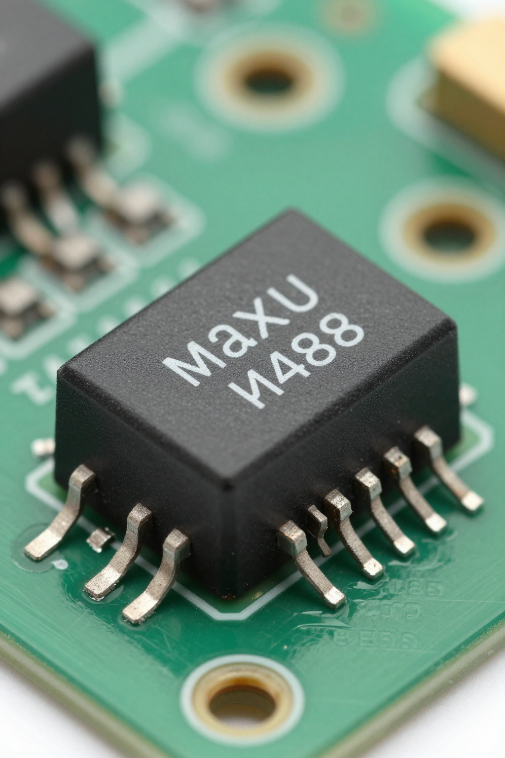
1.1 — What the MAX74821 is (one-line definition + typical spec snapshot)
Point: The MAX74821 is a precision, low‑noise CMOS operational amplifier with rail‑to‑rail input/output behavior intended for low‑power precision signal chains. Evidence: Key typical specs include Vos ≈ 80 µV, input bias current <1 pA, GBW ≈ 10 MHz, slew ≈ 5 V/µs, supply range for single‑supply operation and quiescent current around 1 mA. Explanation: That combination makes the device suitable as front‑end amplifiers, unity‑gain buffers, and active filters where microvolt offsets and low leakage matter.
- Offset (Vos): ~80 µV typical
- Input bias current (Ib): sub‑pA typical
- GBW: ~10 MHz
- Slew rate: ~5 V/µs
- Quiescent current: ~1 mA
1.2 — How to read the datasheet quickly (what pages/figures to scan first)
Point: Scan the absolute‑maximum ratings, the Electrical Characteristics table and the typical performance plots first. Evidence: Absolute limits define survivability; Electrical Characteristics give guaranteed min/max under specified test conditions; typical graphs (noise vs. frequency, output swing versus load, CMRR/PSRR vs. frequency) show expected behavior. Explanation: Prioritize figures showing input bias vs. temperature, input offset drift, and the small‑signal gain/phase plots to assess stability and closed‑loop bandwidth for your intended gain.
2 — Electrical specifications deep-dive: static & dynamic parameters
| Parameter | Symbol | Min | Typ | Max | Unit |
|---|---|---|---|---|---|
| Input Offset Voltage | Vos | - | 80 | 200 | µV |
| Input Bias Current | Ib | - | <1 | 5 | pA |
| Gain Bandwidth Product | GBW | - | 10 | - | MHz |
| Slew Rate | SR | - | 5 | - | V/µs |
| Quiescent Current | Iq | - | 1 | 1.5 | mA |
2.1 — DC specs: offset, bias currents, input/output ranges, CMRR, PSRR
Point: Differentiate typical vs. guaranteed values and inspect test conditions in the datasheet tables to translate specs to system error budgets. Evidence: Offset is often shown as a typical value with separate columns for minimum/maximum over temperature and supply; input bias current is specified under particular source impedance and temperature. Explanation: For precision gain, compute output error = Vos × closed‑loop gain and bias‑current induced error = Ib × source impedance; a 100 µV offset at gain 100 yields a 10 mV output error, while a 1 pA bias into 10 MΩ adds 10 mV, so resistor sizing and guarding are critical.
2.2 — AC specs: gain‑bandwidth, slew rate, noise, settling time, stability
Point: Use GBW and slew‑rate to predict closed‑loop bandwidth and transient behavior. Evidence: The datasheet’s GBW (~10 MHz) and slew (~5 V/µs) combined with open‑loop gain plots determine the maximum gain and bandwidth achievable without peaking; noise density and integrated noise curves set the sensor noise floor. Explanation: For example, a noninverting gain of 10 gives a closed‑loop bandwidth near 1 MHz (GBW/Gain), and slew limits determine the maximum amplitude and edge rate that will be slew‑limited; budget total noise by integrating the noise density over the system bandwidth shown in the datasheet plots.
3 — Pinout, package variants and PCB/layout considerations
3.1 — Pin-by-pin pinout and signal descriptions
Point: Review the official pinout block in the datasheet to map power, inputs, outputs and no‑connects before layout. Evidence: Typical dual/op amp pinouts list V+, V− (or GND), noninverting input, inverting input, output and any NC or substrate pins; the datasheet lists absolute‑maximum voltages per pin. Explanation: Pay attention to which pins are exposed pads or tied to substrate: incorrect connections can raise substrate currents or reduce thermal performance; follow the pin definitions to avoid overdriving inputs beyond input common‑mode limits.
- V+ / VCC — positive supply pin, obey supply range and decoupling.
- V− / GND — negative supply or ground reference; ensure low impedance.
- IN+ — noninverting input; protect from transients, keep traces guarded.
- IN− — inverting input; minimize source impedance and leakage paths.
- OUT — amplifier output; note load drive capabilities and short‑circuit behavior.
- NC / SUB — no‑connect or substrate; leave as recommended by datasheet.
3.2 — Package options, thermal considerations and PCB layout tips
Point: Choose the package consistent with thermal dissipation and assembly constraints. Evidence: Small SOT/SC70 packages reduce thermal mass; the datasheet provides junction‑to‑ambient thermal resistance and recommended land patterns. Explanation: Place the supply decoupling capacitor within 2–5 mm of the V+ pin, use solid ground pours with short return paths, guard sensitive input traces with driven‑guard or ground traces for sub‑pA bias currents, and add thermal vias if the package dissipates more than trivial power in constrained footprints.
4 — Typical applications and concrete design examples
4.1 — Example 1: Low-noise sensor preamplifier
Point: For a transducer with 10 mV/g sensitivity, target a gain of 100 to reach full‑scale ADC range. Evidence: Using Vos ≈ 80 µV and Ib <1 pA, choose feedback resistors that keep Johnson and bias‑induced errors below the amplifier offset contribution; for Rf ~100 kΩ and Rg ~1 kΩ the input noise and bias effects remain manageable. Explanation: Add an RC input filter to limit bandwidth to the sensor bandwidth, protect inputs against ESD and transients with low‑capacitance clamps, and select resistor tolerances such that offset and gain error fit the overall system budget.
4.2 — Example 2: Portable instrumentation / audio buffering
Point: Trading quiescent current and output swing defines battery life and dynamic performance. Evidence: With ~1 mA quiescent current per amplifier, calculate standby drain and estimate active duty cycles; output rail‑to‑rail behavior in the datasheet indicates how close to rails the signal can swing under load. Explanation: For single‑supply audio buffering, ensure the chosen supply and load allow the amplifier to reach required swing with acceptable distortion; where larger capacitive loads exist, include a small series output resistor to maintain stability shown by the datasheet’s load‑stability plots.
5 — Integration checklist, test procedures and troubleshooting
5.1 — Pre-production checklist: what to verify on the bench
Point: Verify power sequencing, decoupling, offset/bias, output swing and stability before committing a layout. Evidence: Bench tests should measure offset (nulling if possible), bias current with high‑impedance source, PSRR/CMRR under expected supply variations and output swing into the anticipated load; use the datasheet tolerances to set pass/fail limits. Explanation: Recommended equipment includes a low‑noise power supply, nanovoltmeter/µV meter, picoammeter or source measure unit, and an oscilloscope for transient and settling measurements; document results against datasheet minima/maxima at room temperature and at worst‑case ambient.
5.2 — Common failure modes and fixes
Point: Instability, unexpected offset drift and thermal issues are common; match symptoms to causes. Evidence: Instability often appears as ringing with capacitive loads; offset drift can correlate with high source impedance or contamination; thermal problems show as gain or offset shifts under load. Explanation: Remedies include adding series isolation resistors at the output for capacitive loads, reducing source impedance or improving guarding to cut bias current‑dependent drift, and verifying package thermal derating and vias to remove excess heat.
Summary
The datasheet numbers — low offset, sub‑pA bias current, modest GBW and low quiescent current — position this op amp for precision, low‑power front ends when layout and test follow the datasheet guidance. Engineers should apply the electrical‑spec calc methods above, validate offset and bias on the bench, and respect pinout and thermal recommendations when placing decoupling and guards.
Next: prototype the reference circuit, run the checklist tests and iterate layout fixes identified during bench validation; consult the datasheet figures and tables referenced earlier when selecting component values and defining pass/fail criteria for production testing.
Key summary
- The MAX74821 excels where microvolt offset and sub‑picoamp bias matter; plan resistor values and source impedance to keep error contributions below the noise floor.
- Read the datasheet electrical tables and typical plots first: absolute‑maximums, guaranteed DC specs and noise/G DW plots directly inform bandwidth and stability choices.
- Layout is critical — place decoupling caps close to supply pins, guard high‑impedance traces, and use thermal vias or pours as the package thermal numbers in the datasheet recommend.
Common questions & answers
How do I measure MAX74821 offset voltage in the lab?
Measure offset by configuring the amplifier as a unity‑gain buffer with inputs shorted or tied to a low‑impedance reference, then read the output with a low‑noise voltmeter. Subtract any buffer gains and divide by closed‑loop gain to calculate input‑referred Vos, and repeat across supply and temperature as guided by the datasheet to verify guaranteed limits.
What are the pinout-related precautions for MAX74821 layout?
Keep supply decoupling within a few millimeters of the supply pin, use a solid ground plane and run sensitive input traces away from digital switching. Guard or driven‑guard high‑impedance inputs, avoid routing input traces under noisy components, and follow the datasheet pinout diagram when assigning exposed pads or NC pins to prevent substrate currents.
How should I test for stability and capacitive load tolerance?
Apply the expected capacitive load plus a range of resistive loads and observe the step response on an oscilloscope. If ringing or overshoot appears, add a small series resistor (10–100 Ω) at the output and re‑test; consult the datasheet’s stability recommendations and repeat settling time and distortion checks after the modification.
Why is input bias current critical for MAX74821 applications?
With sub-pA input bias current, even large source impedances cause minimal offset error. However, board contamination or leakage paths can introduce significant errors. Proper guarding and clean PCB layout are essential to maintain the device's ultra-low leakage advantage in high-impedance sensor interfaces.