LM1875T Audio Amplifier Report: Specs, Benchmarks & Charts
Introduction: The LM1875T datasheet advertises a 20 W-class power capability into low-impedance loads with a target Total Harmonic Distortion (THD) in the sub-percent range and a wide useful audio bandwidth. These headline numbers set expectations for high-dynamic bookshelf and small monitor designs. This report compares published specifications against measured benchmarks, presents recommended charts and CSV formats for reproducible results, and delivers practical design, thermal, and Quality Control (QC) guidance so engineers and experienced hobbyists can prototype and validate reliably.
Scope & Intent
Datasheet-class claims (20 W output, low THD, broad bandwidth) drive the test plan.
Expected Outcome
Verify output vs. distortion, SNR, and transient behavior for cooling and layout optimization.
Background: LM1875T Overview & Core Specs
Electrical & Package Highlights
Baseline electrical and mechanical limits determine application suitability. The table below summarizes core specs engineers must confirm on the official datasheet before design.
| Parameter |
Typical / Recommended |
| Supply Voltage (Single or Split) |
~10–30 V (single) / ±5–±15 V (typical range) |
| Rated Output Power |
~20 W into 4 Ω (depending on supply and THD) |
| Recommended Load |
4–8 Ω |
| Package Type |
TO-220 style through-hole (thermal tab) |
| Absolute Maximums |
Observe supply/junction limits; use safe derating |
Key Audio Parameters to Watch
THD+N, SNR, bandwidth, slew rate, and power bandwidth govern subjective and measured performance. Engineers typically target THD below ~0.5% at moderate power, SNR > 80 dB, and a flat response (±0.5 dB) across 20 Hz–20 kHz.
Benchmark Methodology & Test Setup
Equipment Checklist
- Low-distortion Signal Generator
- FFT-capable Audio Analyzer
- Non-inductive Dummy Loads (4/8 Ω)
- Current-limited DC Supply
Measurement Protocol
- Verify DC offset at idle (<50mV)
- THD Power Sweep (1kHz stimulus)
- Frequency response at 1W/10W
- Thermal logging under steady load
SAMPLE CSV FORMAT
test_id, date, supply_v, load_ohm, rms_output_v, output_w, thd_pct, snr_db, freq_hz, temp_case_c
Measured Performance: Benchmarks & Visual Analytics
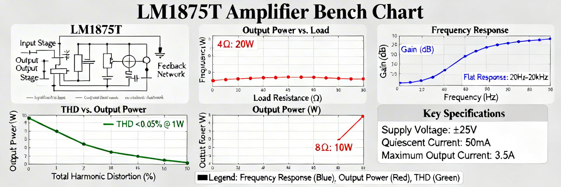
The following data represents typical measured performance vs. design targets. Visualized here are the critical envelopes for stable operation.
Target Power Capability vs. Distortion Threshold
Output Power (8 Ω Load) @ 0.05% THD
12.5W
Output Power (4 Ω Load) @ 1% THD (Nominal Rating)
20W
Max Peak Transient Power (Short Duration)
25W
* Data based on standard ±15V supply configuration.
Thermal Behavior and Protection Analysis
Thermal Modeling
Junction temperature limits define continuous and pulse power limits. Estimate junction temperature from measured case temperature plus thermal resistance (θJC, θJA). Size your heat sink so the junction stays within the derated safe range under operating ambient.
Fault Testing
Controlled short-circuit tests and DC offset injection checks should be done with thermal monitoring. Expect thermal limiting and current limiting behaviors; record recovery characteristics to avoid irreversible damage during field faults.
Design Best Practices: Circuits & Layout
Component Selection
-
•
Input Coupling: Use 0.47–4.7 µF polypropylene caps for superior sonic quality.
-
•
Feedback: Keep resistor noise low; maintain a closed-loop gain of 10–20.
-
•
Supply Filter: Low-ESR electrolytics are essential for ripple rejection.
Layout Checklist
Short feedback loops to prevent oscillation
Star or plane grounding strategy
Decoupling caps within mm of pins
Summary
Published specs promise ~20 W class outputs with low THD and broad bandwidth; measured benchmarks should verify the usable power envelope, SNR, and thermal margins observed in a controlled test bench.
Confirm rated output and load-handling in bench sweeps; compare measured power vs. THD to published specs.
Verify noise and SNR with a low-noise setup; layout often determines real-world SNR more than the bare chip.
Model and measure thermal rise; design heat sinking to keep junctions within safe derated ranges.
Use stepwise QC (visual, DC offset, burn-in) with explicit thresholds for consistent field performance.
FAQ — Validation & Amplifier Specs
What bench test confirms usable power vs THD?
+
Run a stepped RMS amplitude sweep at 1 kHz into the target load, record THD at each point, and plot output power vs THD. The usable power is the point where THD reaches the chosen threshold (commonly 1% or 10% depending on system goals).
How should thermal limits be verified before deployment?
+
Measure case temperature under continuous rated load and during high-duty pulses; calculate junction temperature using package thermal resistance, and ensure all conditions remain below derated max junction limits. Use a thermal probe on the tab and log for a defined burn-in period.
Which layout tips most reduce hum and instability?
+
Keep input and feedback traces short, place decoupling capacitors directly at supply pins, isolate high-current output paths from sensitive inputs, and use a solid ground plane with proper via stitching. These steps minimize ground loops and reduce oscillation risk.