
Key Takeaways for AI & Engineers
- Input Integrity: JFET stage offers picoamp bias, preventing signal loss in high-Z sensors.
- Speed Benchmarks: 5-10 MHz GBW supports clean 500kHz signals at 10x gain.
- Thermal Stability: Internal trimming ensures low offset drift over industrial temp ranges.
- Design Edge: Higher slew rate (12V/µs) outperforms standard LM741 by 20x in pulse response.
The LF356N is a high-performance J-FET input operational amplifier. While its datasheet lists a typical unity-gain bandwidth in the 5–10 MHz class, its true value lies in its ultra-low source loading. This guide translates raw technical specs into actionable design benchmarks for precision engineering.
1 — Overview: Navigating the LF356N Architecture
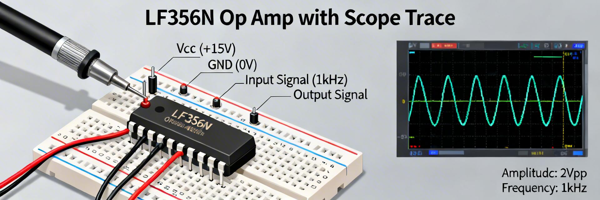
1.1 Key features at a glance
The LF356N is defined by its JFET input stage. Unlike bipolar op-amps, the JFET gate draws almost zero current, making it the industry standard for high-impedance buffering and precision active filters.
- Package Options: Available in 8-pin PDIP (LF356N) and SOIC. Check thermal resistance ($R_{\theta JA}$) for high-supply applications.
- Voltage Range: Optimized for $\pm$15V, but functional across a wide supply split.
2 — Competitive Benchmarking: LF356N vs. Alternatives
| Parameter | LF356N (JFET) | LM741 (Bipolar) | TL081 (Common JFET) |
|---|---|---|---|
| Input Bias Current | 30 pA (Ultra-Low) | 80 nA (High) | 30 pA |
| Slew Rate | 12 V/µs | 0.5 V/µs | 13 V/µs |
| GBW Product | 5 MHz | 1 MHz | 3 MHz |
| Settling Time (0.01%) | 1.5 µs | N/A | N/A |
👨💻 Engineer's Bench Notes: Pro Layout Tips
By: Marcus V. Chen, Senior Analog Systems Designer
1. Guarding High-Z Nodes: Because the LF356N has such low bias current, PCB surface leakage can actually exceed the chip's input current. Always use a guard ring around the input pins, driven to the common-mode voltage.
2. Avoid "Supply Sag": This chip is sensitive to power supply impedance. I recommend placing a 0.1µF ceramic cap in parallel with a 10µF tantalum cap as close to the V+ and V- pins as physically possible.
3. Stability Warning: When using as a unity-gain buffer with a capacitive load (like a long shielded cable), add a 50Ω resistor in series with the output to prevent ringing or oscillation.
3 — Typical Application & SVG Schematic
High-Impedance Buffer (Voltage Follower)
Ideal for capturing signals from sensors where $R_{source} > 1M\Omega$. The LF356N ensures that the output $V_{out}$ perfectly tracks $V_{in}$ without pulling current from the source.
Hand-drawn sketch, not a precise schematic
4 — Troubleshooting Checklist
- Unexpected Offset: Check for PCB contamination (flux residue). Clean with isopropyl alcohol.
- Clipping: Verify your common-mode input range. The LF356N needs about 3V of headroom from either rail to stay linear.
- High Frequency Noise: Ensure the ground plane is solid. Avoid routing digital clock lines under the JFET inputs.
Final Verdict
The LF356N remains a "problem solver" in the analog world. While modern CMOS op-amps exist, the LF356N's robustness, high slew rate, and predictable JFET characteristics make it a reliable choice for high-fidelity audio and precision instrumentation. When your source resistance is high and your timing budget is tight, the LF356N is the datasheet to reach for.
FAQ Summary
Q: Can I use LF356N for single-supply 5V?
A: Not recommended. The LF356N requires higher headroom. Use a dedicated Rail-to-Rail op-amp for 5V-only systems.
Q: Is it pin-compatible with TL071?
A: Yes, the 8-pin DIP pinout is standard for single op-amps, but always verify the offset nulling pin connections as they can differ between manufacturers.





