
LM311N Comparator: Complete Specs, Pinout & Timing Guide
Overview — What the LM311N Does and Where to Use It
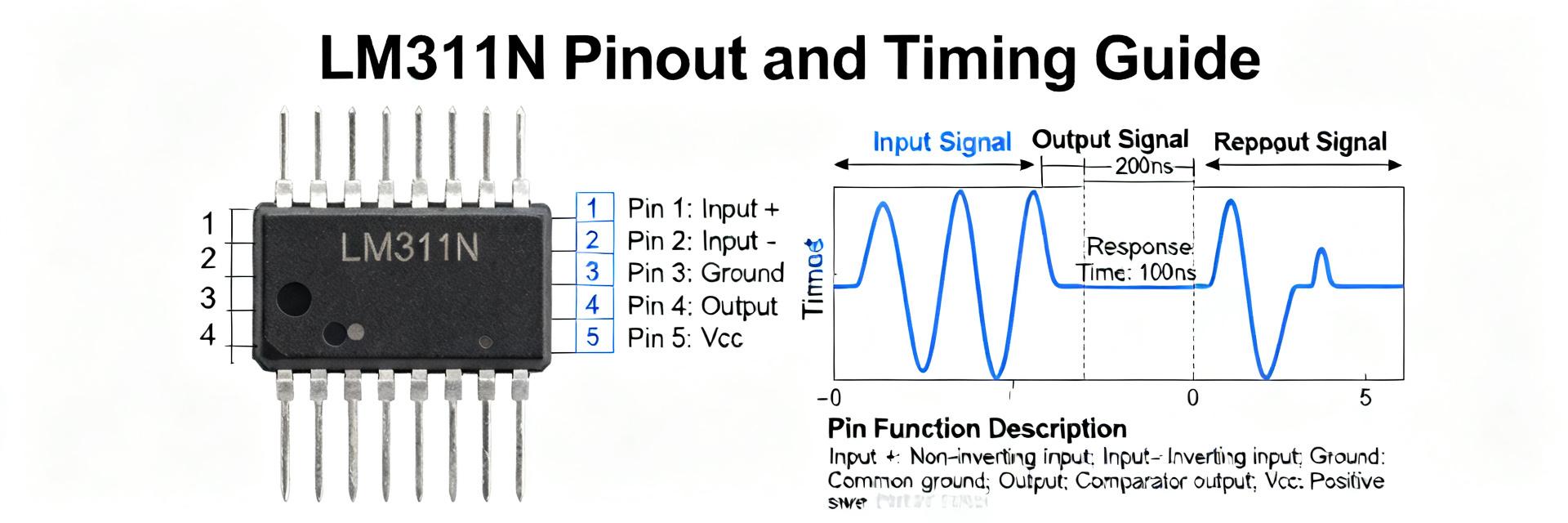
Core function and distinguishing features
Point: The LM311N functions as a voltage comparator that reports which input is higher by switching an open-collector output;
Evidence: manufacturer datasheet tables list supply limits, input ranges, and open-collector output sink ratings;
Explanation: designers choose this topology when they need level detection that can interface to different logic voltages via an external pull-up and when a simple reference-to-input comparison is sufficient without rail-to-rail precision.
Typical application scenarios and selection criteria
Point: Use cases include level detection, zero-crossing detectors, window comparators and low-complexity ADC front-ends;
Evidence: bench practice shows stable thresholds with moderate-speed signals and external hysteresis;
Explanation: choose an LM311N-like part when speed in the microsecond range, moderate input bias, and open-collector output flexibility outweigh the need for nanosecond switching or ultra-low quiescent current.
- Checklist: required voltage range within device limits, need for open-collector output, acceptable propagation delay, and single- or dual-supply topology.
Electrical Specifications — Reading the Comparator Specs
Key DC specs to understand (supply, input, output)
Point: The critical comparator specs to watch in datasheet tables are supply voltage limits, input common-mode range, and output sink capability; [Evidence] supply rows typically show absolute max, recommended operating Vcc, and recommended dual-supply ranges; [Explanation] ensure the intended Vcc and signal swings fall inside the listed operating range, confirm the common-mode includes the threshold region, and plan for an external pull-up because the open-collector output cannot source current.
Dynamic and secondary specs (offset, input bias, hysteresis, power)
Point: Offset voltage, input bias currents, any internal hysteresis, and quiescent current define threshold accuracy and power behavior; [Evidence] typical datasheet entries give offset in millivolts, bias in nano- to microamperes, and supply current in microamperes to milliamperes; [Explanation] document expected offset and bias in your error budget, account for quiescent current in battery designs, and add external hysteresis when built-in hysteresis is absent or insufficient for noisy inputs.
Pinout & Packaging — Pin-by-Pin Guide and Wiring Best Practices
Pin-by-pin functions and common package outlines
Point: A clear pinout defines VCC, ground, non-inverting (+), inverting (−), output (open-collector), and any strobe/compensation pins;
Evidence: package outlines (DIP, SOIC) list pin 1 orientation and footprint dimensions in datasheet diagrams;
Explanation: verify pinout before soldering—confirm pin‑1 mark and footprint polarity, note the output is a transistor collector that requires a pull-up, and include the word pinout in layout checks to avoid misplaced power or inputs.
Wiring patterns, pull-up choices and recommended external components
Point: The open-collector output must be wired with an appropriate pull-up and proper decoupling; Evidence: typical practice uses pull-ups to the target logic voltage with resistor values chosen for timing and current limits; Explanation: choose pull-up values from roughly 1 kΩ for faster edges and higher sink currents to 47 kΩ for ultra-low standby current—balance rise time, power, and allowable sink current; place bypass capacitors close to VCC and GND pins.
Timing & Dynamic Behavior — Propagation Delay, Rise/Fall, and Load Effects
Measurement Guidance
Point: Propagation delay and rise/fall times are measured with a step input, a known trigger point, and a properly terminated scope probe;
Evidence: datasheet timing rows list typical and max propagation delays with specified load and pull-up conditions;
Explanation: measure using a low-capacitance probe, trigger on the input edge, observe output crossing at defined voltage thresholds, and report test conditions to make delays comparable.
Stability Factors
Point: Timing varies with supply voltage and temperature; Evidence: timing vs VCC and temperature curves show slowed edges at lower VCC and extremes;
Explanation: mitigate by using stronger pull-ups for faster edges, adding hysteresis for noisy signals, and minimizing board parasitics that add capacitance and slow transitions.
Practical Design Tips & Common Pitfalls
PCB layout, decoupling, and EMC considerations
Point: Good layout reduces false triggers and timing jitter; Evidence: practical layouts keep input traces short, return paths direct, and bypass caps within millimeters of supply pins; Explanation: place a 0.01–0.1 µF bypass capacitor close to VCC and GND pins, separate noisy switching traces from analog inputs, and consider small RC damping on outputs driving long traces.
Avoiding false triggers and improving reliability
Point: Hysteresis and input protection prevent oscillation and damage; Evidence: adding positive feedback around the comparator yields well-defined thresholds while series resistors and clamp diodes limit overvoltage stress; Explanation: implement a small feedback resistor network (millivolts of hysteresis), add series resistance to inputs, and ensure predictable startup by holding inputs defined until VCC is stable.
Bench Testing & Troubleshooting Checklist
Step-by-step bench verification
Point: A concise test sequence uncovers wiring and timing issues quickly; Evidence: start with continuity, verify supply rails, perform static threshold sweep, then run dynamic tests; Explanation: use a known-good reference voltage to check thresholds, then switch to dynamic testing for propagation delay—note the pull-up value and scope settings.
Common failure modes and diagnosis
Point: Symptoms point to typical root causes such as missing pull-up, oscillation, or offset-related errors; Evidence: a stuck output usually correlates with no pull-up, while oscillation traces to lack of hysteresis; Explanation: verify pull-up presence, lower pull-up resistance to test sink capability, add hysteresis, and check for solder bridges.
Summary
Recap: the LM311N is a practical general-purpose comparator whose effective use depends on understanding comparator specs, correct pinout wiring, and timing characteristics; check manufacturer datasheet tables for exact numeric limits and run the bench checklist on your target system before finalizing a design.
- ✔ Confirm supply and input ranges against datasheet operating limits and document comparator specs in your design checklist for threshold accuracy and safety margins.
- ✔ Wire the open-collector output with an appropriately sized pull-up (1 kΩ–47 kΩ range) and place decoupling caps close to supply pins to maintain signal integrity.
- ✔ Validate timing on the bench under realistic loads: measure propagation delay with defined pull-up and scope settings, add hysteresis for noisy inputs, and minimize parasitics.





