
In bench comparisons, mid-speed low-power comparators with sub-100 ns propagation delays typically enable noticeably faster threshold detection and tighter window control than general-purpose parts, reducing detection latency by measurable percentages in fast power-management loops. This article delivers concise datasheet highlights, the practical metrics engineers should measure, design tips, and an integration checklist for TLV1831QDCKRQ1 for engineers, hardware designers, and buyers.
The focus is pragmatic: what the datasheet prioritizes, which lab benchmarks expose real-world behavior, PCB and input-conditioning guidance, and a compact QA checklist to validate parts before production. Terms used include comparator and datasheet to align with procurement and validation workflows.
1 — Background: What the TLV1831QDCKRQ1 is and where it fits
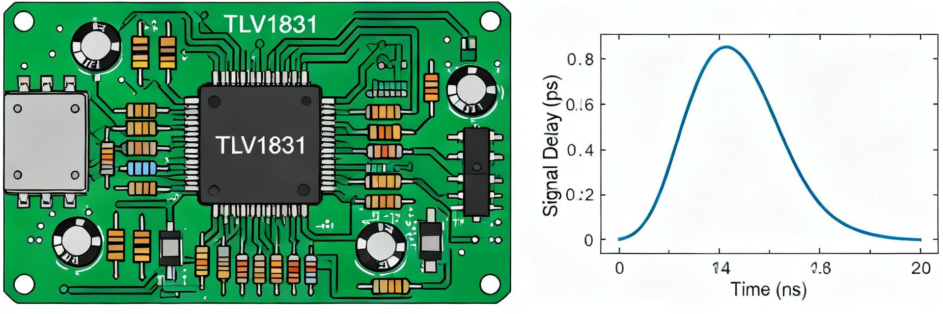
1.1 — Device class & intended applications
Point: The TLV1831QDCKRQ1 is a single-channel, general-purpose comparator optimized for low-voltage systems where size and low quiescent current matter. Evidence: It targets threshold detection, window comparators, level sensing, and simple power-sequencing roles. Explanation: Designers pick it over bulkier comparators when footprint, single-supply operation, and a balance of speed versus power are primary constraints.
1.2 — Package & operating conditions
Point: The device is offered in a very small 5-pin package (DCK-equivalent) suitable for dense PCBs and limited-space modules. Evidence: Typical temperature grading supports industrial ranges (roughly −40°C to 125°C). Explanation: For thermal derating, keep traces short, place bypass caps close to VCC, and consider thermal vias if the layout concentrates multiple dissipating parts.
2 — Key datasheet metrics for TLV1831QDCKRQ1
2.1 — Electrical specs to prioritize
Point: Prioritize supply range, input common-mode, output type, and quiescent current when reading the datasheet for TLV1831QDCKRQ1. Evidence: The part supports low-voltage single-supply operation, rail-to-rail input behavior, and a push-pull output option, with microamp-class quiescent current typical. Explanation: Wide low-voltage support simplifies single-supply designs, rail-to-rail inputs ease input-divider choices, and low ICC preserves standby battery life.
2.2 — Timing & accuracy metrics
Point: Key timing specs include propagation delay, input offset, and hysteresis options. Evidence: Family figures place propagation delay comfortably under 100 ns in many conditions; offset and hysteresis define switching stability. Explanation: Read timing tables with the specified VCC, input step, and load; propagation delay often increases near the supply rails and under heavier output loads.
3 — Performance benchmarks & practical measurements
3.1 — Typical lab benchmarks to run
Point: Run propagation delay vs. VCC, input offset vs. temperature, output drive into defined loads, idle and switching supply current, and common-mode rejection tests. Evidence: Report VCC, input amplitude, load resistor, and temperature for each metric. Explanation: Consistent test conditions (e.g., VCC steps, 100 mV to 2 V input steps, defined RL) make results comparable across lots and validate datasheet claims in your system.
3.2 — Expected trade-offs & graph recommendations
Point: Expect speed‑vs‑power trade-offs and degraded rail-to-rail performance near supply extremes. Evidence: Typical trade-offs show faster propagation at higher VCC with increased dynamic current. Explanation: Include propagation-delay vs VCC, offset vs temperature, and a supply-current histogram (idle vs switching) to visualize operating envelopes in publications or design reviews.
4 — Design & implementation best practices
4.1 — PCB layout and decoupling
Point: Decoupling and routing strongly affect comparator stability and jitter. Evidence: Use a 0.1 μF ceramic bypass close to VCC pin and a 1 μF bulk nearby, keep input traces short, and reference inputs to the same ground plane as the comparator. Explanation: Short input leads reduce pickup; good bypassing prevents supply transients from translating into false toggles.
4.2 — Input conditioning and hysteresis strategies
Point: For noisy signals, add hysteresis and simple RC filtering. Evidence: Typical positive-feedback resistor ranges from 100 kΩ to 1 MΩ for millivolt-scale hysteresis; RC time constants depend on event bandwidth. Explanation: Implement input clamping (diodes or series resistors) for over-voltage protection and choose hysteresis to suppress chatter while preserving required sensitivity for the application—comparator guidance remains central to robust designs.
5 — Typical use cases & comparisons
5.1 — Example circuits
Point: Two compact circuits illustrate common roles: a battery undervoltage threshold detector and a pulse conditioner/zero-cross detector. Evidence: For battery undervoltage, use a simple resistor divider to create threshold and a 100 kΩ–1 MΩ hysteresis leg; expected latency ~tens of ns to low‑100 ns. Explanation: The small package and rail-to-rail input make the part ideal where board space and single-supply simplicity are required.
5.2 — How it compares to nearest alternatives
Point: Compared to other low-voltage fast comparators, the trade axes are speed, supply range, quiescent current, and package. Evidence: Expect competitive propagation delay and lower standby current at the cost of limited feature sets (no internal reference). Explanation: Authors should include a short table comparing these axes for clarity when recommending the part relative to similar families.
6 — Buying & integration checklist
6.1 — Pre-purchase checklist
Point: Confirm supply range, temperature grade, package, output type, and lead-free/assembly options with procurement. Evidence: Request sample quantities and traceable marking for initial evaluation. Explanation: Early confirmation of package code and temperature grade prevents last-minute surprises during assembly or compliance testing.
6.2 — Quick integration QA checklist
Point: On-silicon and board-level verification ensure integration success. Evidence: Bench-test propagation delay, offset, supply current, perform thermal soak, and validate final PCB under real loads. Explanation: Cross-check measured values against the datasheet and record conditions to build a production acceptance plan and reduce field failures.
| Parameter | Summary |
|---|---|
| Supply voltage (VCC) | Low-voltage single-supply operation (typical 2.7 V–5.5 V range) |
| Temperature range | Industrial-grade (~−40°C to 125°C) |
| Propagation delay | Family figures: sub-100 ns, often ~60–80 ns under moderate conditions |
| Output type | Push-pull (rail-friendly) suitable for direct logic drive |
| Package | Small 5-pin DCK-equivalent footprint for dense PCB layouts |
Summary
The TLV1831QDCKRQ1 stands out for compact footprint, rail-to-rail input capability, low quiescent current, and competitive propagation delay—attributes valuable in battery-powered and space-constrained designs. Designers should prioritize bench checks that validate timing, offset, and supply behavior under expected loads before committing to production.
- Compact, low‑power comparator behavior: small package and low ICC make this comparator suitable for space- and energy-limited designs; validate quiescent and dynamic currents in your system.
- Timing matters: propagation-delay vs VCC and load determines usable latency; measure delay across your VCC range and record conditions for production acceptance.
- Layout and conditioning: follow tight decoupling, short input traces, and add hysteresis/RC filtering for noisy signals to prevent false switching in real systems.
Frequently asked questions
What are the typical propagation-delay expectations for TLV1831QDCKRQ1?
Under moderate loads and nominal VCC, expect propagation delays in the tens of nanoseconds up to under 100 ns. Measure with your target load and supply; propagation delay typically shortens at higher VCC while dynamic current increases. Document test conditions for repeatability.
How should a designer verify comparator datasheet claims during prototyping?
Run controlled bench tests: propagation delay vs VCC, input offset vs temperature, output drive into the intended load, and both idle and switching supply currents. Use consistent signal amplitudes and document load, temperature, and probe impedance to compare against datasheet values.
What PCB-layout and decoupling practices reduce comparator-induced noise?
Place a 0.1 μF ceramic bypass close to the VCC pin and a 1 μF bulk cap nearby, keep input traces short and routed away from high-current loops, and reference inputs to a low-impedance ground plane. Add series resistors or small RC filters on sensitive inputs to suppress high-frequency transients.
What advantages do the rail-to-rail input and push-pull output design offer?
The rail-to-rail input configuration simplifies input divider sizing across varying signal levels, while the push-pull output allows direct, high-efficiency logic drive without requiring external pull-up resistors, conserving board space and system power.





