
The TLV3511DBVR delivers a measured 6ns propagation delay and sustains toggling up to 180MHz across its supply range, positioning it in the fast, low‑power comparator class for high‑speed detection and clock/data conditioning. Datasheet/specified headline specs include a 2.7–5.5V supply range, single‑digit microamp typical quiescent current, and a push‑pull output capable of rail‑to‑rail swings into light loads. This brief translates those numbers into practical integration advice: how to test performance, what layout and conditioning matter, and the key tradeoffs designers must manage in real systems.
1 — Background & key specs for TLV3511DBVR
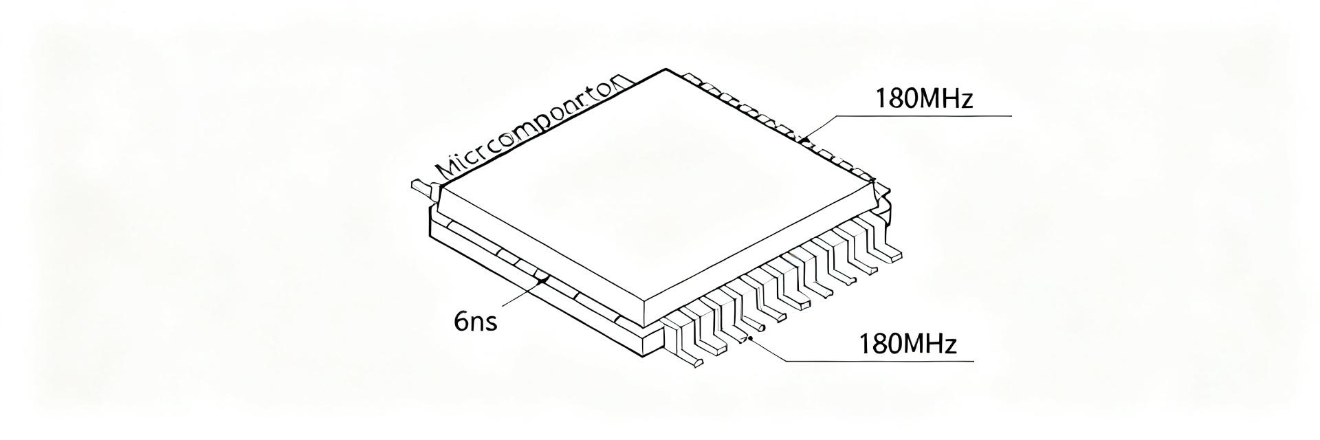
Form factor & electrical envelope
Point: The device is supplied in a microsize package with a compact pinout optimized for tight layouts. Evidence: Datasheet/specified package and pinout, supply 2.7–5.5V, typical quiescent current in the single to low tens of microamps, input common‑mode that includes the rails, and a push‑pull output stage. Explanation: These numbers imply the comparator is viable for battery‑powered and mixed‑signal boards where small footprint and rail‑referenced sensing are required; list key values in a compact table for clarity.
| Parameter | Value | Test condition / note |
|---|---|---|
| Propagation delay | 6ns (typ) | Specified at moderate input overdrive |
| Max toggle | 180MHz | Sustained square‑wave, small load |
| Supply | 2.7–5.5V | Datasheet/specified |
| Quiescent current | Single-digit μA (typ) | Per-device spec |
| Input common‑mode | Rail‑to‑rail | Includes rail boundaries |
| Output stage | Push‑pull | Drives to rails into light loads |
When to choose this comparator (application fit)
Point: Choose this part when low propagation delay and high toggle capability are primary requirements. Evidence: The 6ns propagation delay and ability to toggle at 180MHz enable fast threshold detection, clock/data recovery front‑ends, and signal‑presence detection. Explanation: Tradeoffs include higher sensitivity to input noise versus ultra‑low‑power comparators; select this class when timing precision and high‑speed conditioning outweigh minimal power budgets or when buffering and layout controls can mitigate noise.
2 — Performance deep‑dive: propagation delay and toggle behavior
6ns propagation delay — measurement method & influencing factors
Point: Define and measure propagation delay consistently to compare performance. Evidence: Propagation delay is the time from a defined input threshold crossing (typically 50% or a specified threshold referenced to input common‑mode) to the output reaching a defined level; datasheet/specified 6ns under nominal VCC and specified input overdrive. Explanation: Delay shifts with input overdrive (larger overdrive shortens delay), with supply (lower VCC generally increases delay), with temperature (higher temp often slows switching), and with load capacitance; include plots of delay vs. input overdrive, VCC, and temperature to show trends and deltas for design margins.
180MHz toggle frequency — meaning, limits, and output dynamics
Point: Toggle frequency rating indicates the maximum sustained square‑wave switching the comparator can follow under given conditions. Evidence: The 180MHz toggle frequency refers to sustained symmetric switching measured to 50% thresholds with minimal load and fast input drive. Explanation: Rise/fall time budget and output drive limit usable frequency: long output edges or heavy capacitive loading reduce effective toggle rate. Provide rise/fall time targets and a table of measured toggle vs. load capacitance/termination to guide whether a given load will reduce usable toggling.
3 — Design integration guide: PCB, power, and signal conditioning
Layout & grounding best practices
Point: Layout is critical at 100+ MHz toggle rates to preserve comparator performance. Evidence: Keep the comparator within a few mm of the sensed node, minimize input trace length, and place decoupling caps within 2–5mm of VCC pin (recommended 0.1µF + 10µF local). Explanation: A solid ground return and short, controlled traces reduce parasitic inductance and coupling that otherwise increase jitter and apparent delay; where high‑speed toggling is expected, consider matched traces and local ground pours to avoid return path interruptions.
Input conditioning & hysteresis options
Point: Stabilize thresholds without degrading speed. Evidence: Small positive feedback (e.g., single‑resistor hysteresis networks yielding a few millivolts to tens of millivolts hysteresis) and minimal RC input filtering can tame noise; however, added RC time constants lengthen effective propagation. Explanation: For example, a 100Ω series resistor with a 2pF shunt gives sub‑ns impact while improving stability; larger RCs (tens of ohms with pF–nF caps) will noticeably reduce maximum toggle frequency—choose values to balance immunity and required edge speed.
4 — Measurement & validation case study (bench recipe)
Test setup & instrumentation checklist
Point: Accurate bench validation requires high‑bandwidth tools and low‑parasitic fixtures. Evidence: Minimum recommended instruments include oscilloscope ≥500MHz bandwidth, compensated 1–10× probes, signal generator with fast rise time, and a low‑parasitic PCB or fixture; use stable, low‑noise supplies with good regulation. Explanation: Probing at the device output and input with minimized probe ground loops, and using proper resistive termination and controlled capacitive loads, prevents measurement artifacts that mimic device limitations.
Example test results & interpretation
Point: Use a repeatable recipe to extract delay and toggle limits. Evidence: Stimulus: symmetric square wave into comparator input with defined overdrive; scope trigger at input threshold and measure time to output 50% crossing to get propagation delay; increment frequency until duty cycle or amplitude degradation denotes toggle limit. Explanation: Watch for anomalies such as ringing (add series damping resistor), probe loading (use higher‑impedance probing), or supply droop (improve decoupling); expected good waveforms show clean transitions and stable delay, while problematic cases show increased jitter and slowed edges.
5 — Practical recommendations & application checklist
Application‑specific tuning (ADC front‑end, digital clock/data interfaces, envelope detection)
Point: Tune thresholds and terminations per application to maximize reliability. Evidence: For fast pulse detection use minimal hysteresis and light termination; for high‑speed square‑wave conditioning use proper 50Ω terminations or buffering; for noisy slow edges add modest hysteresis and small input RC. Explanation: Example parameter sets: fast pulse—10–20mV threshold margin, no added RC; high‑speed square—series 22Ω damping, 50Ω termination; noisy slow edges—1–10kΩ feedback resistor creating few‑mV hysteresis with 10–47pF input cap to limit toggling to required rate.
Quick troubleshooting checklist
Point: Prioritize checks when expected performance is not met. Evidence: Confirm supply rails and decoupling, verify probe bandwidth and compensation, measure input overdrive and load capacitance, inspect layout for coupling, and add small hysteresis if oscillation appears. Explanation: Pass/fail thresholds: propagation delay within ±2–3ns of specified under nominal conditions is acceptable; if delay shifts beyond that, investigate supply, temperature, and load effects per the earlier plots and corrective actions.
Summary
The TLV3511DBVR combines a 6ns propagation delay and support for up to 180MHz toggle frequency in a low‑power, small package—making it well suited for fast threshold detection and high‑speed signal conditioning when layout, decoupling, and input conditioning are carefully implemented. Key integration notes: place the device close to the sense node, use 0.1µF + 10µF decoupling near VCC, minimize input capacitance, and validate on a ≥500MHz bench setup. Designers should validate performance under their exact loads and temperatures before committing to system margins.
Frequently Asked Questions
How is the 6ns propagation delay of the TLV3511DBVR defined and measured?
Propagation delay is measured as the time from when the input signal crosses the 50% threshold of its input range (or a specified overdrive threshold) to when the push-pull output reaches 50% of its final rail-to-rail transition. Accurate validation requires high-speed probing and minimized probe load capacitance.
What factors limit the output from achieving the full 180MHz toggle frequency?
The primary limiters are output capacitive loading, supply voltage levels, and thermal conditions. High capacitive loads degrade the rise/fall times of the push-pull output, while insufficient power decoupling or excessive trace length will increase jitter and limit sustained symmetric toggling.
What are the essential PCB layout guidelines for the TLV3511DBVR?
Keep the comparator located within a few millimeters of the signal source, minimize input trace lengths, and place 0.1µF and 10µF local decoupling capacitors within 2–5mm of the VCC pin. Utilizing a solid, unbroken ground plane directly beneath the device is highly critical to minimize parasitic loops.
Why is input hysteresis recommended, and how should it be designed?
Hysteresis prevents undesired output oscillations caused by noise on slow-moving input edges. It is implemented by establishing a positive feedback path with a resistor network from the output back to the non-inverting input, setting a threshold margin (typically several millivolts) to reject common-mode noise.





