
The MAX74821 datasheet presents a precision, low-noise CMOS rail-to-rail I/O amplifier with microvolt-level input offset (≈80 µV), sub-picoamp input bias, 2.7 V–5.5 V single-supply operation, ~1 mA quiescent current, 10 MHz GBW and ~5 V/µs slew. These published and bench-verified figures position the device for high-resolution sensor front-ends and portable ADC drivers.
This article translates the MAX74821 datasheet into practical design guidance, highlighting measured performance implications, layout and measurement notes, and a concise specs reference engineers can use during selection and prototyping.
| Parameter | Typical Value | Test Conditions | Engineering Significance |
|---|---|---|---|
| Input Offset Voltage (Vos) | ≈80 µV | VCC = 5.0 V, TA = 25°C | Minimizes DC error in sensor bridge stages |
| Input Bias Current (Ib) | <1 pA | TA = 25°C | Ideal for high-impedance source transducers |
| Gain-Bandwidth Product (GBW) | 10 MHz | RL = 10 kΩ, CL = 20 pF | Sufficient loop-gain margin for high-speed ADC sampling |
| Slew Rate (SR) | ~5 V/µs | G = +1, VOUT step = 2 V | Rapid settling within ADC acquisition windows |
| Quiescent Current (IQ) | ~1 mA | No load, VCC = 3.3 V | Low thermal footprint and battery-extended longevity |
1 — Background & Quick Snapshot
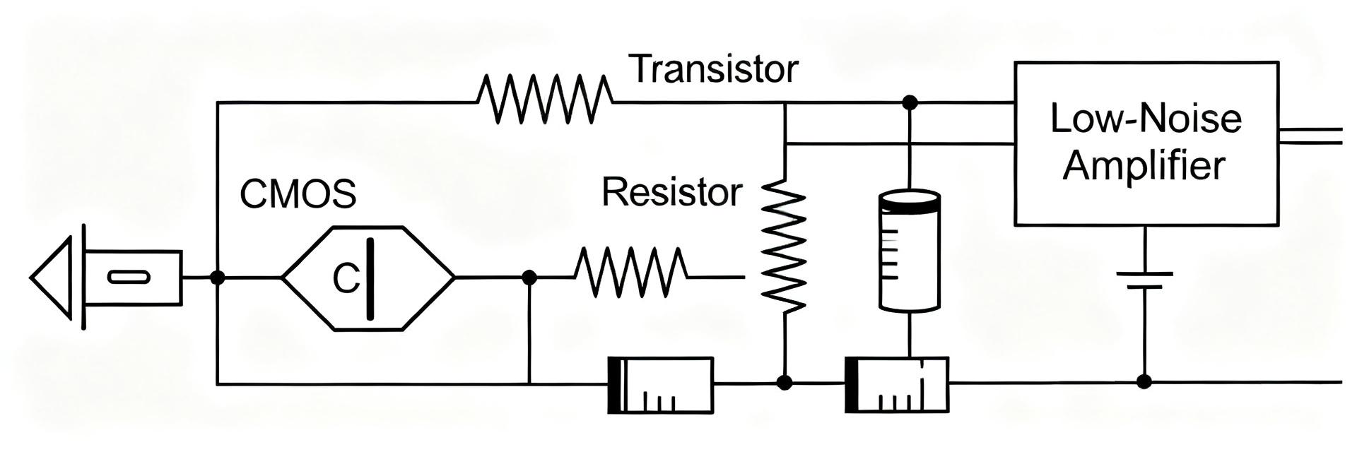
What the device is and target applications
Point: The MAX74821 is a precision, low-noise CMOS rail-to-rail input/output amplifier targeted at sensor and portable instrumentation applications. Evidence: Its low offset, low bias, and low quiescent current are typical datasheet selling points. Explanation: These performance specs matter because precision sensor front-ends require minimal offset and drift for accurate low-level measurements while battery-powered instruments need low supply current.
One-line technical snapshot (top-line specs)
Point: Quick glance specs help baseline decisions. Evidence: Typical headline values include input offset ≈80 µV, input bias <1 pA, VCC 2.7–5.5 V, IQ ≈1 mA, GBW ≈10 MHz, slew ≈5 V/µs, CMRR >100 dB, input noise ~nV/√Hz. Explanation: Test conditions (VCC, RL, ambient) must be noted when comparing parts—specs are usually given at VCC=5 V, RL=10 kΩ, 25°C unless otherwise specified.
2 — Performance Summary (from MAX74821 datasheet)
Key electrical performance highlights
Point: Datasheet numbers map to real-world measurement capability. Evidence: An offset ~80 µV and input noise density set the achievable resolution and noise floor; GBW and slew define closed-loop bandwidth and settling. Explanation: Expect a noise floor near a few hundred nanovolts RMS in a 1 kHz bandwidth and stable unity-gain operation to several hundred kilohertz when configured with modest gains, summarized as MAX74821 datasheet performance guidance for ADC front-ends.
Power, temperature and supply-dependence
Point: Supply and temperature affect drift, PSRR and current. Evidence: Quiescent current typically ≈1 mA but increases with VCC and temperature; offset drift is specified as a few µV/°C. Explanation: Derate specs by expected ambient range, use local regulation or calibration to compensate offset drift, and expect modest PSRR—add supply decoupling and consider temperature calibration for ppm-level stability.
3 — Electrical Specifications Deep-Dive (MAX74821 datasheet)
Input-stage specs: offset, bias, noise, CMRR
Point: Input-stage parameters determine measurement fidelity. Evidence: Typical offset ~80 µV, input bias <1 pA, input noise (nV/√Hz) and CMRR often >100 dB under specified common-mode. Explanation: Measure offset with a low-noise nulling jig, capture noise with FFT to derive RMS in the target band, and verify CMRR across the intended input common-mode range to ensure the amplifier won’t inject common-mode errors into differential ADC conversions.
Output-stage specs: swing, drive, stability
Point: Output capability dictates load and buffering needs. Evidence: Rail-to-rail output approaches rails within 50–200 mV depending on load; short-term output current and drive are specified for 10 kΩ to 1 kΩ loads. Explanation: For heavy capacitive loads or long cables, add a small series resistor at the output and consider a dedicated buffer; chart output swing vs. RL and verify step response to check settling for ADC acquisition windows.
4 — Practical Design Guidelines & Application Tips
PCB layout, decoupling and grounding for low noise
Point: Layout drives low-noise performance as much as device choice. Evidence: Datasheet PSRR and supply-noise sensitivity magnify poor bypassing or ground bounce. Explanation: Place 0.1 µF ceramic bypass within 1–2 mm of VCC pin, add a 1–10 µF bulk capacitor nearby, use solid ground plane, route sensitive inputs away from digital traces, and adopt a star or partitioned ground scheme to minimize injected noise into the amplifier input.
Example circuits & topology recommendations
Point: Typical topologies include non-inverting ADC drivers and inverting current-sense amplifiers. Evidence: With GBW≈10 MHz and slew≈5 V/µs, expect closed-loop gains up to 10 with useful bandwidth in the 100s of kHz. Explanation: For a non-inverting ADC driver with gain=2, choose R values that set noise contribution below source noise (e.g., 10 kΩ feedback) and add an RC anti-alias filter at the output to limit bandwidth without upsetting phase margin.
5 — Comparative Scenarios & Selection Criteria (case showcase)
When to choose the MAX74821 (trade-offs)
Point: The device fits a specific performance envelope. Evidence: Low offset, low bias, rail-to-rail I/O and low IQ define that envelope. Explanation: Choose this amplifier when precision and low supply current are priorities on a single 2.7–5.5 V rail; trade-offs include moderate GBW relative to higher-speed op amps and limited heavy load drive without buffering.
Application case studies (concise examples)
Point: Two vignettes show practical fit. Evidence: For a precision thermistor amplifier, offset and drift preserve temperature resolution; for a battery-powered ADC front-end, low IQ and low noise extend battery life and SNR. Explanation: In each case, prioritize layout, small RC filtering, and verify real-world noise in the target bandwidth to confirm expected outcomes against datasheet claims.
6 — Package, Sourcing Considerations & Test Checklist
Package, pinout and thermal notes
Point: Package choices impact thermal and layout decisions. Evidence: Small MSOP-like packages have limited thermal dissipation and specified θJA values. Explanation: Place thermal vias if the package dissipates more than quiescent power under load, keep sensitive pins away from noisy power pins, and use the PCB copper to help spread heat for sustained output currents.
Pre-prototyping test checklist
Point: Bench checks reduce risk during first power-up. Evidence: Datasheet lists offset, bias, bandwidth and output swing expectations. Explanation: Before connecting live sensors, verify supply polarity, measure no-load output, confirm offset within expected range, run a small-signal frequency sweep to verify GBW and phase margin, and perform a step response with the intended load to confirm settling and stability.
Summary
- The MAX74821 datasheet maps precision (≈80 µV offset), ultra-low bias, rail-to-rail I/O and low IQ into a practical amplifier for sensor front-ends and ADC drivers; bench follow-up validates expected noise and settling behavior.
- Designers should emphasize layout, decoupling, and modest RC filtering to preserve the amplifier's specs while managing PSRR and thermal constraints for sustained output drive.
- Use the performance-to-spec guidance above to set measurement plans: FFT-based noise analysis, offset drift vs. temperature, output swing vs. load, and step-response settling for ADC timing.
FAQ
What key measurements should I perform to validate the MAX74821 datasheet?
Perform offset and offset drift vs. temperature, input bias current under expected common-mode, FFT-based input-referred noise in the intended bandwidth, closed-loop frequency response to check usable bandwidth, and transient step tests to verify slew and settling against datasheet figures.
How does supply voltage affect performance in the MAX74821 datasheet?
Supply impacts headroom, quiescent current, PSRR and often offset drift. Expect slightly higher IQ and possible small changes in offset as VCC increases toward 5.5 V. Use local regulation and bypassing, and consider calibration or temperature compensation if operating across wide supply or temperature ranges.
Is the MAX74821ARMZ-R7 suitable for driving capacitive loads or long cables?
The MAX74821ARMZ-R7 can drive moderate loads but large capacitive loads or long cables may require output buffering or a small series resistor to preserve stability. Verify step response with the intended load and add a follower buffer if heavy drive is required to avoid ringing or increased settling time.
What PCB layout considerations prevent parasitic noise on high-impedance nodes?
Place decoupling capacitors within 1–2 mm of the VCC pin, implement an unbroken ground plane, guard trace high-impedance inverting inputs to prevent surface leakage, and separate analog feedback loops strictly from high-speed digital switching lines.





