
Translating datasheet numbers into practical engineering limits prevents surprises in prototype and field testing. This deep dive focuses on the INA299 and the published datasheet entries, quantifying typical margins engineers must apply so lab behavior matches system expectations under transient and steady conditions.
Field cross-checks often reveal a 10–40% gap between nominal numbers and usable margins; that gap matters for safety, accuracy, and reliability. The analysis below converts headline specs into actionable rules, test procedures, and integration checklists so designers can move from spec sheet to validated design margins.
1 — Device overview & headline specs (Background)
1.1 What the INA299 is and common applications
Point: The device is a bidirectional current-sense, precision front end for low-side or high-side sensing. Evidence: It conditions small differential voltages across a sense resistor and produces a scaled output compatible with ADC inputs. Explanation: Typical roles include power-rail monitoring, battery-management sensing, and motor-drive feedback in embedded systems; target users are embedded and power-design engineers.
1.2 Headline datasheet numbers to call out
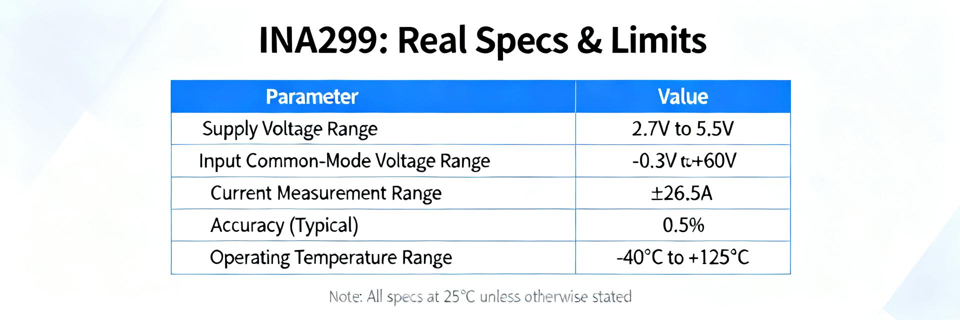
Point: Pulling the most relevant specs into a compact reference saves repeated lookups. Evidence: The table below lists headline specs you will use in margin calculations and test plans. Explanation: Keep this table adjacent to lab notes so each bench test cites the same baseline values from the datasheet and your validation results.
| Spec name | Datasheet value (typical) | Location (datasheet) |
|---|---|---|
| Allowed common-mode range | -0.1 V to 120 V | Electrical characteristics |
| Survival voltage | ±140 V (transient) | Absolute maximum ratings |
| Input offset | ~25 µV typical | Input specs |
| Input bias | <1 nA typical | Input specs |
| CMRR | ≥100 dB (low freq) | AC/DC characteristics |
| Gain-bandwidth (GBP) | ~1.1 MHz | Dynamic specs |
| Small-signal bandwidth | ~200 kHz | Dynamic specs |
| Quiescent current | ~0.5 mA | Supply characteristics |
2 — Operating envelope: voltages, currents, thermal (Data analysis)
2.1 Interpreting common-mode vs survival voltage
Point: Distinguish continuous common-mode operating range from survival limits used for transients. Evidence: Operating range defines guaranteed accuracy; survival limits permit no functional damage if briefly exceeded. Explanation: Design protections—TVS diodes, series resistors, careful sense-resistor placement—must constrain expected transients to the survival window and keep steady-state CM inside the operating range for accurate readings.
2.2 Current, power dissipation, and thermal constraints
Point: Sense-resistor choice sets voltage, power, and thermal stress. Evidence: Use P = I²·R for resistor dissipation; device heating depends on package thermal resistance and board conduction. Explanation: Example: with Rsense = 0.05 Ω and I = 5 A, P = 1.25 W in the resistor; ensure resistor and nearby copper can remove that heat and verify device junction rise stays within derating curves to avoid thermal overstress.
3 — Accuracy and dynamic specs: offset, CMRR, bandwidth (Data analysis)
3.1 DC accuracy: offset, offset drift, input bias, gain error
Point: DC error budget determines usable low-current limits. Evidence: Measurement error combines input offset, offset drift over temperature, input-bias induced voltage across Rsense, and gain error. Explanation: Example: with R = 0.1 Ω and I = 10 mA, signal is 1 mV. An offset of 50 µV is a 5% error; add gain error and bias-induced error to compute total uncertainty and set minimum measurable current.
3.2 AC behavior: gain-bandwidth, small-signal bandwidth, and CMRR vs frequency
Point: Dynamic specs limit transient fidelity. Evidence: GBP and small-signal bandwidth determine rise time and settling; CMRR typically falls with frequency. Explanation: Estimate 10–90% rise time ≈ 0.35 / bandwidth; for 200 kHz bandwidth, expect ~1.75 µs. On switching rails, reduced CMRR at higher frequency injects CM error into the differential measurement—use filtering or synchronous sampling to mitigate.
4 — Failure modes and limits: what breaks first (Method/guide)
4.1 Typical failure triggers (overvoltage, reverse CM, thermal overstress)
Point: Failures are usually caused by abuse beyond survival specs. Evidence: Common triggers include sustained out-of-range common-mode, reversed CM during hot-plug, or excessive package junction temperature. Explanation: These modes lead to input breakdown, latch-up, or long-term drift; prioritize protective components and consider derating for continual reliability in hostile environments.
4.2 How to test failure limits safely (bench procedure)
Point: Controlled bench tests reveal practical thresholds without destroying multiple parts. Evidence: Start with gradual ramps and pulsed transients while logging waveforms, currents, and temperature. Explanation: Use isolation, current-limited sources, and incremental steps of 5–10% toward absolute ratings; stop and inspect for performance degradation, then increase only if prior step passed all checks.
- Set baseline: verify nominal operation and record offsets, gain, and temp.
- Ramp CM voltage in 5–10% increments, log differential output and leakage.
- Inject pulsed transients (short duty) up to survival rating; inspect for permanent shift.
- Thermal soak: hold elevated ambient and repeat steps, watching for drift.
5 — Measurement validation: replicating datasheet numbers (Method/guide + Case)
5.1 Test setups to reproduce datasheet conditions
Point: Reproduce the datasheet test environment to compare like-for-like. Evidence: Match supply voltages, decoupling, ambient temperature, load, and measurement bandwidth stated in the datasheet. Explanation: Use differential probes or isolated ADC inputs, short ground returns, and place decoupling capacitors per recommendations to avoid probe or layout artifacts that bias results.
5.2 Common discrepancies and how to explain them
Point: Lab values often differ due to bandwidth, layout, or measurement method. Evidence: Typical causes include insufficient decoupling, long sense traces, probe loading, or different test temperatures. Explanation: Troubleshooting checklist: reduce probe bandwidth, shorten traces, add recommended input caps, and re-measure; document each change so you can correlate correction magnitude with the observed discrepancy.
- Check probe grounding and use a differential probe.
- Validate test bandwidth vs datasheet figure conditions.
- Apply recommended decoupling and layout fixes incrementally.
6 — Integration checklist & design rules (Actionable recommendations)
6.1 Design checklist: layout, filtering, protection, and sense resistor sizing
Point: Layout and component choices make the spec usable in the system. Evidence: Star ground, short sense traces, and local decoupling improve accuracy. Explanation: Filter with RC time constants tuned to the application; choose Rsense so I·Rsense yields a measurable voltage while keeping power dissipation and error under target percentage; verify protection components respect survival limits.
- Sense trace: shortest possible, with single-point return to ADC ground.
- Decoupling: close to device supply pins, 0.1 µF + 1 µF recommended.
- Protection: series resistor and transient suppressor sized to clip transients within survival ratings.
6.2 Quick decision flow & derating rules
Point: Decide when to accept datasheet values versus derate and test. Evidence: For low-risk, non-safety circuits, limited derating (≈20%) is often acceptable; for safety-critical or harsh environments, derate 30–40% and run full failure testing. Explanation: When in doubt, apply the “test-first” rule: build the validation jig, perform failure-limit bench procedures, and publish measured margins for design sign-off. Use long-tail phrases such as “INA299 common-mode survival limit test” and “INA299 measurement accuracy at low currents” in lab reports.
Summary
- The INA299 headline specs give a starting point, but designers should derate operating margins (20–40%) and verify thermal and CM behavior under expected transients; always document measured vs datasheet numbers for traceability.
- Key measurement rules: reproduce datasheet test conditions, use differential probing, and budget a combined error of offset, bias, and gain when sizing sense resistors to meet accuracy targets.
- Run controlled failure tests (CM ramp, pulsed transients, thermal soak) before relying on nominal specs; the recommended next step is to build the validation jig described above and report measured vs datasheet performance.
Frequently Asked Questions
What practical margin should I apply to INA299 common-mode and survival specs?
Apply a conservative derating of 20–40% depending on risk: 20% for benign environments, 30–40% for hot, noisy, or safety-critical systems. Confirm by pulsed-transient tests and thermal soak so the applied margin reflects measured, not just nominal, capability.
How do I validate INA299 measurement accuracy at low currents?
Recreate datasheet conditions: same Rsense, supply decoupling, ambient temp, and bandwidth. Use a low-noise current source, differential probe, and compute total error = offset + (Ibias·Rsense) + gain error. Adjust Rsense until measured uncertainty meets your percent target.
What bench steps confirm INA299 failure limits safely?
Baseline performance first, then increment CM in 5–10% steps while logging differential output, leakage, and temperature. Inject short, controlled transients up to survival ratings with current-limited supplies, inspect for permanent offset shifts, and repeat under thermal soak to find practical failure thresholds.
Why do lab measurements differ from datasheet headline specs?
Lab values often differ due to bandwidth, layout parasitics, insufficient decoupling, long sense traces, probe loading, or different test temperatures. Use differential probes and local decoupling to align lab findings with published numbers.





