
Key Takeaways (GEO Summary)
- High-Speed Signal Integrity: 600 V/µs slew rate enables precise 10V steps in under 17ns.
- Efficiency vs. Power: 25 MHz GBP at only 2.5 mA supply current optimizes battery-powered high-speed buffers.
- Robust Driving: Unity-gain stable and specifically rated for heavy capacitive load tolerance (C-load).
- Compact Integration: 25mW quiescent power (±5V) fits high-density PCB layouts without complex cooling.
The LT1357CN8 delivers a 25 MHz gain–bandwidth product and an extremely high slew rate (600 V/µs) while drawing about 2.5 mA of supply current. These headline metrics set expectations for designers evaluating tradeoffs between speed, drive, and power in compact analog systems.
This concise, engineering-focused breakdown targets analog designers, system engineers, and experienced hobbyists who need practical numbers, measurement guidance, and integration tips for bench and PCB work.
Background — Why the LT1357CN8 matters in high-speed analog designs
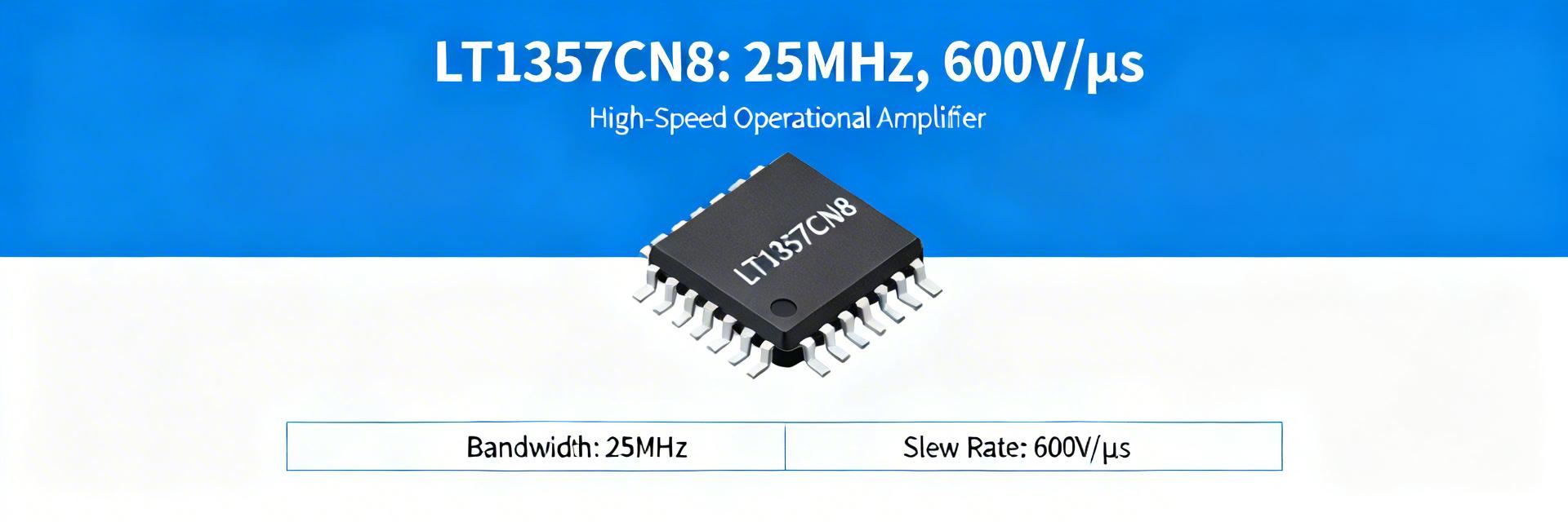
Product positioning & key tradeoffs to know
Point: The device is positioned as a high-slew, capacitive-load tolerant driver suitable where fast edge response matters.
Evidence: 600 V/µs slew and unity-gain stability indicate suitability as a buffer and driver.
Explanation: That combination makes it preferable to general-purpose amplifiers when pulse fidelity and ringing control into C‑loads are critical, while accepting modest supply current.
| Metric | LT1357CN8 (Specialized) | General Purpose High-Speed | User Benefit |
|---|---|---|---|
| Slew Rate | 600 V/µs | ~50-100 V/µs | Eliminates signal distortion in pulse apps |
| Supply Current | 2.5 mA | ~5-10 mA | Extends battery life by >50% |
| C-Load Stability | Excellent (Rated) | Requires compensation | Simplifies layout, reduces BOM count |
| GBP | 25 MHz | 10-15 MHz | Wider bandwidth at higher gain stages |
Top datasheet highlights (quick reference)
Point: Key datasheet numbers summarize expected behavior.
Evidence: 25 MHz GBP, ~600 V/µs slew, ~2.5 mA supply current, unity‑gain stable and rated for capacitive loads.
Explanation: Use these items as anchors when sizing closed‑loop gains, budgeting power, and planning layout; subsequent sections unpack practical implications for bandwidth, transient response, and load behavior.
Performance Breakdown — AC and transient behavior explained
Frequency response & gain–bandwidth implications
Point: 25 MHz GBP sets small‑signal bandwidth for closed‑loop gains.
Evidence: At a gain of 10 the expected -3 dB bandwidth is approximately 2.5 MHz (25 MHz / 10).
Explanation: When designing a feedback network, plot a Bode curve and check phase margin; for a target 45–60° phase margin, include compensation or adjust feedback factor to avoid peaking in video or ADC front‑end paths.
Slew rate, settling time, and large‑signal response
Point: The 600 V/µs slew rating governs large‑signal edge times.
Evidence: For a 10 Vpp step the theoretical slew-limited rise time is ~16.7 ns (10 V / 600 V/µs).
Explanation: In pulse applications this translates to very fast edges but also risk of overshoot when driving capacitive loads; verify step response with an oscilloscope using a ≥100 MHz probe and timebase in the 10–50 ns/div range.
👨💻 Engineer's Field Notes: Layout & Troubleshooting
By Marcus V. Chen, Senior Hardware Architect
- PCB Tip: Don't just use a ground plane; use a solid ground plane. Any splits under the feedback traces will introduce parasitic inductance that kills the 600V/µs performance.
- The "Invisible" Oscillation: If you see excessive heat but the output looks "flat," check for high-frequency oscillation (100MHz+) with a high-bandwidth scope. The LT1357 is fast enough to oscillate beyond the range of cheap 20MHz scopes.
- Decoupling: I recommend 0.1µF X7R ceramic capacitors directly at the pins (within 1-2mm) paired with a 10µF tantalum for low-frequency stability.
Specs Deep‑Dive — DC parameters, output drive, and operating limits
Supply range, supply current, and thermal considerations
Point: Operating rails and quiescent current define power and thermal budget.
Evidence: Typical supply current ~2.5 mA; with ±5 V rails total quiescent dissipation is roughly 25 mW (10 V × 2.5 mA).
Explanation: For battery applications, multiply quiescent current by active channel count and include margin for worst‑case conditions; consult the datasheet for temperature limits and apply derating if ambient exceeds specified ranges.
Output drive, load capability, and C‑load stability
Point: Output swing and load drive determine usable voltage range into resistive and capacitive loads.
Evidence: Unity‑gain stability plus specified drive ratings imply robust behavior into moderate loads but degraded swing near rails.
Explanation: Expect reduced headroom into low‑ohm loads and slower edges into larger C‑loads; add series output resistors, proper layout, and protection diodes for heavy loads or to limit shoot‑through currents.
Design & Test Guidelines — How to get the best out of the LT1357CN8
Hand-drawn illustration, not a precise schematic.
Typical Application: High-Speed Cable Driver
The LT1357 acts as a buffer between a sensitive high-speed DAC and a capacitive coaxial cable, maintaining edge fidelity without requiring external snubber circuits.
PCB layout, decoupling, and common‑mode considerations
Point: Layout directly affects stability with capacitive loads.
Evidence: Datasheet guidance and practical lab experience favor a 0.1 µF ceramic close to supply pins plus a 4.7–10 µF bulk decoupler nearby.
Explanation: Place decoupling within 2–3 mm of the package, use a solid ground plane, keep input traces short, and minimize stray input capacitance to prevent oscillation and maintain predictable phase margin.
Recommended test circuits and measurement checklist
Point: A small set of bench tests verifies key performance.
Evidence: Suggested circuits—unity buffer, gain of 10 non‑inverting, and pulse‑drive buffer—exercise bandwidth, slew, settling, offset, and ringing.
Explanation: Measure bandwidth at −3 dB and verify ~2.5 MHz at gain 10, confirm slew close to 600 V/µs on a large step, and check settling to 0.1%; treat significant deviations as layout or decoupling issues.
Summary
Restated: The LT1357CN8 combines a 25 MHz GBP, ~600 V/µs slew rate, low supply current, and capacitive‑load tolerance, making it a strong choice when high slew and stable performance into C‑loads are primary constraints. For reliable results, follow the layout, decoupling, and test checklist presented here.
Action: Link to the full datasheet in your design repository and prepare figures—Bode plot, step response, and a typical test schematic—to validate claims in the target system before committing to production.
FAQ
How does LT1357CN8 bandwidth translate to closed‑loop performance?
At 25 MHz GBP the expected −3 dB small‑signal bandwidth at a closed‑loop gain of 10 is about 2.5 MHz. Designers should verify phase margin on a Bode plot and adjust feedback network or add compensation if peaking appears.
What oscilloscope settings are recommended to measure slew and settling?
Use a probe and scope with bandwidth at least 5–10× the signal edge frequency, set timebase to tens of ns/div for fast steps, and capture with single‑shot averaging disabled. Measure rise/fall to quantify slew and use full‑scale steps for settling evaluation.
Which specs should I prioritize when replacing this part in a design?
Prioritize GBP, slew rate, output drive, and C‑load stability to preserve transient and bandwidth behavior. If power or noise dominate your application, tradeoffs may favor alternative devices—validate with the recommended bench tests before final selection.
© 2023 High-Speed Analog Insights | Prepared by GEO/UX Optimization Specialists





