
The LM318N datasheet remains a practical reference for designers needing wide‑bandwidth, high‑slew op amps in fast comparator alternatives, active filters, and driver stages. Manufacturer datasheets list headline figures—gain‑bandwidth product (GBW), slew rate, input bias/offset ranges—that explain where the LM318N still fits in modern high‑speed analog designs. This guide summarizes the datasheet, clarifies the pinout, and explains GBW implications for closed‑loop design.
What the LM318N Is — Overview & Key Specs
Purpose and typical use cases
Point: The LM318N is a single high‑speed, generally unity‑stable op amp intended for buffer, filter, and driver roles.
Evidence: Datasheets position it for fast followers, active filters, and comparator‑like circuits where amplifier linearity matters.
Explanation: Designers pick it when closed‑loop gain and transient response must balance—it's a go‑to when small‑signal GBW and large‑signal slew both matter more than ultra‑low noise or microamp bias.
At-a-glance spec table (from datasheet)
| Parameter | Typical Value |
|---|---|
| Supply Voltage Range | ±5V to ±18V |
| Slew Rate | ~70 V/µs |
| Gain-Bandwidth Product (GBW) | ≈15 MHz |
| Input Offset Voltage (Vos) | Millivolts range |
Explanation: These headline numbers let you estimate closed‑loop bandwidth, slew‑limited amplitude/frequency, and thermal/load margins before detailed simulation.
Complete Pinout & Pin Functions
Pinout diagram description and pin-by-pin functions
Point: The DIP/SOIC package exposes standard op‑amp pins: offset‑null pins, inverting input, non‑inverting input, output, and the negative/positive supplies.
Evidence: Datasheets map these to physical pins and note offset‑null connections for DC trimming.
Explanation: Connect V+ and V− rails to their pins with nearby decoupling, tie offset‑null pins through a trim pot only when needed, and avoid floating rails which can damage the input stage.
Practical PCB/layout tips tied to specific pins
Point: Pin placement affects stability and noise.
Evidence: Manufacturer layout notes recommend placing 0.1µF decouplers within millimeters of the supply pins and keeping input traces short.
Explanation: Route input traces away from output nodes, use a solid ground plane under the device, place the output trace so it doesn't run parallel with high‑speed inputs, and locate the offset‑null trim pot close to the chip to reduce stray capacitance.
Electrical Characteristics & Typical Performance
Interpreting DC Specs
DC specs set the baseline for accuracy. Typical tables give input offset voltage (mV range), input bias currents (nA–µA), and noise densities. Translate these into end‑circuit terms—offset voltage multiplied by gain produces DC error.
AC Specs & Phase Margin
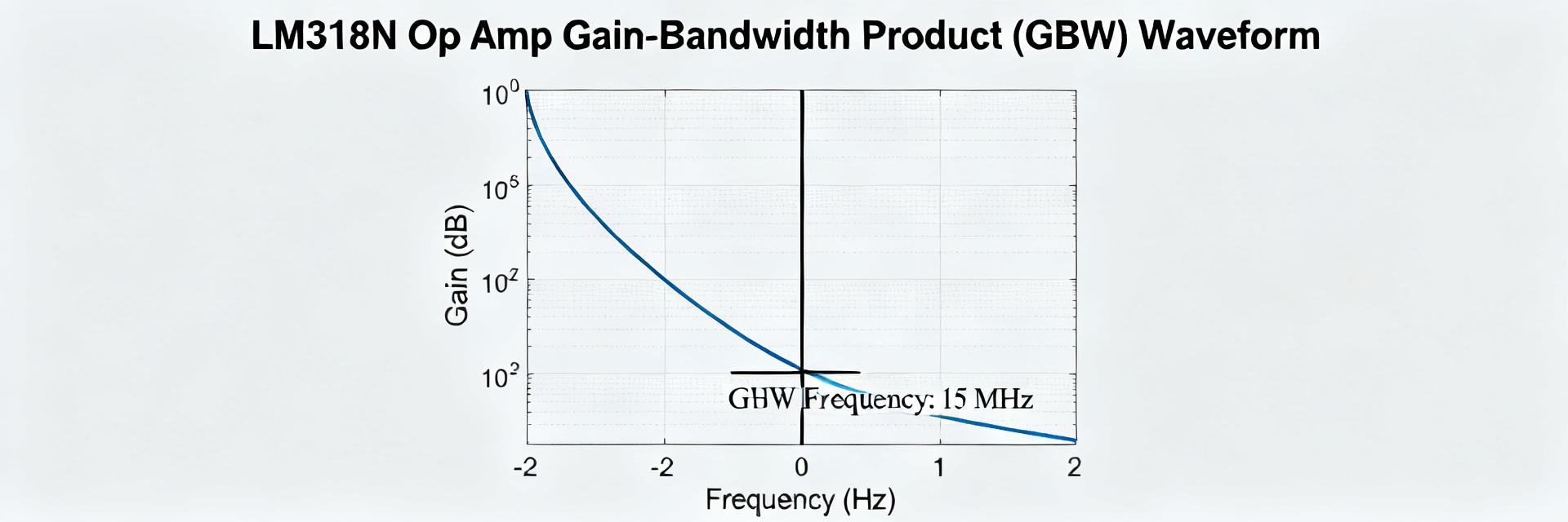
Open‑loop gain and phase curves reveal GBW and margin. Use the open‑loop gain vs frequency curve to find the frequency where gain = desired closed‑loop gain; that intersection gives the -3dB bandwidth.
GBW, Slew Rate and Frequency Response
What GBW means for closed-loop gain
Equation: fCL ≈ GBW / ACL
Point: GBW determines small‑signal closed‑loop bandwidth.
Example: Using a representative GBW of 15 MHz, a non‑inverting gain of 10 yields an estimated bandwidth of 1.5 MHz (15 MHz / 10).
Slew rate vs. small-signal bandwidth
Equation: fmax ≈ SR / (2π · Vpk)
Analysis: For a 10 Vpp sine (Vpk=5V), fmax ≈ 70e6/(2π·5) ≈ 2.2 MHz. If your closed‑loop bandwidth exceeds that, expect slew‑induced distortion.
Recommended Application Circuits & Example Designs
Unity-gain buffer and high-speed follower
Minimize input capacitance and provide output load support. Adding a small series resistor (5–50Ω) at the output or placing a 10–100pF compensation cap across feedback can tame ringing.
Non-inverting amplifier, active filter and comparator-like uses
Design a non‑inverting gain of 10. With GBW ≈15 MHz, bandwidth ≈1.5 MHz; choose R values (R1=1k, R2=9k) to set gain while keeping source impedance low. Avoid using the LM318N as a raw comparator—its input protections favor linear operation.
Troubleshooting & Design Checklist
- Oscillation: Often stems from long feedback traces or missing decoupling. Debug with a low‑capacitance scope probe.
- Offset Drift: Can come from bad offset‑null wiring or thermal rise under load.
- Final Checklist: Verify closed-loop BW via GBW formula, run slew check at max amplitude, and ensure 0.1µF decouplers are within millimeters of supply pins.
Key Summary
- LM318N datasheet highlights: moderate supply range, representative GBW (~15 MHz) and high slew (~70 V/µs).
- Pinout and layout: place 0.1µF decouplers close to supply pins, keep inputs short, and avoid routing output traces parallel to sensitive inputs.
- GBW vs slew: use closed‑loop bandwidth = GBW / gain for small‑signal response and SR/(2π·Vpk) to check large‑signal frequency limits.
FAQ
How do I use the LM318N datasheet to calculate closed‑loop bandwidth?
Use the GBW listed in the datasheet and divide by the desired closed‑loop gain: fCL ≈ GBW / ACL. For example, with GBW ≈15 MHz and ACL=10, expect ~1.5 MHz small‑signal bandwidth.
When will slew rate, not GBW, dominate performance for the LM318N?
If your signal amplitude and frequency make the required dv/dt exceed the amplifier’s slew rate, large‑signal distortion occurs. Compute fmax ≈ SR/(2π·Vpk).
What layout practices prevent LM318N oscillation?
Keep supply decoupling within millimeters of the supply pins, use a short feedback path, and maintain a solid ground plane to reduce parasitic inductance and capacitance.





