
Across hobbyist and industrial designs, the LM324 family remains a go-to quad op amp for single-supply applications — its datasheet-driven specs (input range, output swing, quiescent current) explain why. This guide explains how to read a typical datasheet, interpret the pinout, extract key specifications, and use charts and bench checks to design and troubleshoot with confidence.
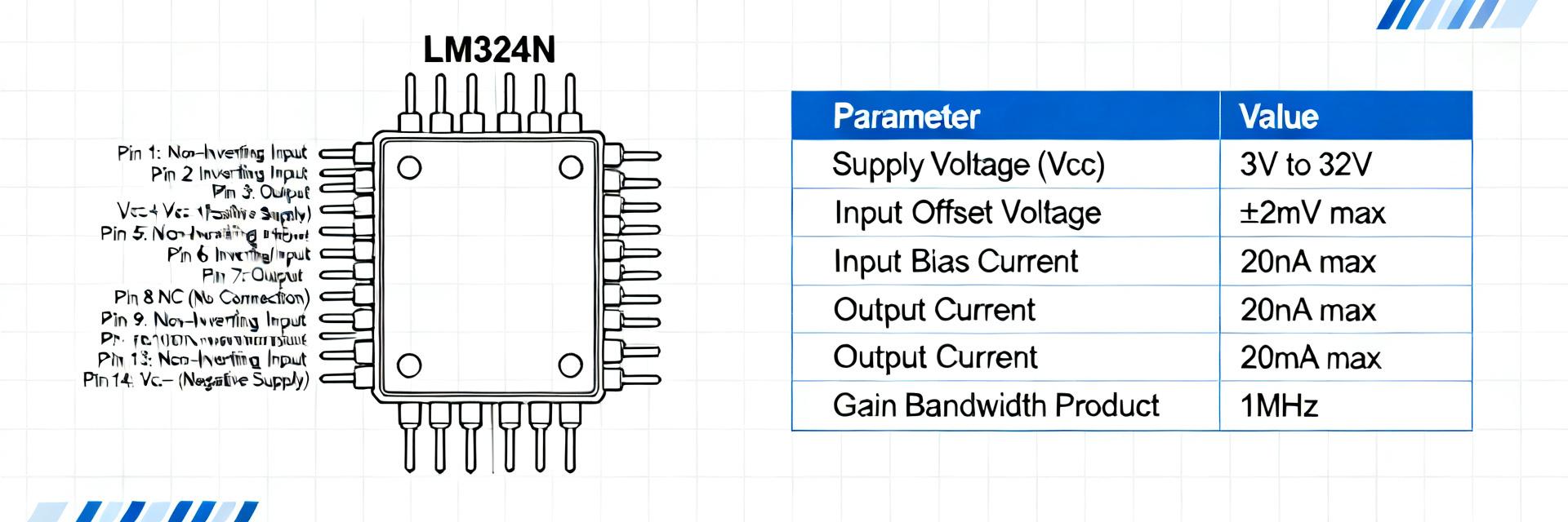
LM324N Overview: What the Datasheet Tells You
Core device description & package options
The device is a quad operational amplifier optimized for single-supply operation with low quiescent current per amplifier, making it suitable for battery-powered and general-purpose analog front-ends. Typical packages include DIP and SOIC variants; the datasheet front page lists ordering codes, device family summary and absolute maximum ratings such as supply-voltage and input pin limits.
At-a-glance spec table (must-have quick reference)
| Parameter | Typical / Range | Notes |
|---|---|---|
| Supply range | +3V to +32V (single) / ±1.5V to ±16V | Guaranteed limits on datasheet |
| Input common-mode | V– to (V+ – 1.5V) | Not rail-to-rail |
| Output swing | V– + ~20mV to V+ – ~1.5V | Load dependent |
| Gain-bandwidth | ~1 MHz | Typical performance |
| Input offset | ~2–7 mV | Check max in table |
| Input bias | ~20–200 nA | Temperature dependent |
| Iq per amp | ~40–80 µA | Ultra-low power |
Electrical Characteristics Deep Dive
Input & differential specs
Read the electrical table for input offset voltage (typical and max), input bias current, and common-mode voltage limits. Offset and bias values affect low-frequency accuracy and DC stability; common-mode limits determine whether inputs can reach the negative rail in single-supply designs.
Pinout & Typical Connections
Pin-by-pin functional notes
Pin mapping varies with package; typical quad layout lists four amplifier blocks with two inputs and one output each plus V+ and V– power pins. Tie unused inputs to a defined voltage (ground or mid-rail) via resistor or bias network to avoid floating.
| Pin | Function |
|---|---|
| 1 / 7 / 8 / 14 | Outputs (A, B, C, D) |
| 2 / 6 / 9 / 13 | Inverting Inputs (-) |
| 3 / 5 / 10 / 12 | Non-inverting Inputs (+) |
| 4 | V+ (Positive Supply) |
| 11 | V– (Ground / Negative Supply) |
Design Checklist & Troubleshooting
- Decoupling: Place 0.1µF capacitors within 5mm of V+ pins.
- Unused Amps: Configure as followers with non-inverting input to ground.
- Capacitive Loads: Use a 100Ω series resistor to prevent oscillation.
- Headroom: Ensure input signal stays 1.5V below V+ rail.
Frequently Asked Questions
What are the essential datasheet checks for LM324N before design?
Check absolute maximum supply limits, input common-mode range, output swing under expected load, input offset and bias specifications, and quiescent current per amplifier. These determine headroom and DC accuracy in your configuration.
How can I verify output swing and offset on the bench?
Measure output swing by configuring the amp as a follower and driving its input near expected extremes while applying the intended load. For offset, short the inputs in a unity buffer and measure output error voltage.
What quick fix if the amplifier oscillates in my circuit?
Add a small series resistor (50–200Ω) at the output to isolate capacitive loads, add 0.1µF decoupling at supplies, shorten input trace lengths, and verify supply stability.
Is the LM324N rail-to-rail?
No. The input common-mode range typically goes to the negative rail (GND in single supply) but stays ~1.5V below the positive rail. The output also swings close to GND but cannot reach VCC.
Summary: LM324N datasheet guidance is critical for avoiding stability pitfalls. Always prioritize supply decoupling and respect the common-mode input window for reliable industrial performance.





